


Contents

On-demand webinar
How Good is My Shield? An Introduction to Transfer Impedance and Shielding Effectiveness
by Karen Burnham
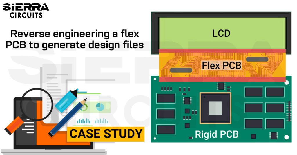
Our PCB design engineers reverse-engineered a flex circuit to recreate the design files and optimize the LCD connectivity. The FPC connected the LCD display and the main rigid circuit board.
Since the client didn’t possess the design files, we had to redesign the board to generate the Gerber files to get the board manufactured.
In this case study, you’ll learn how our design engineers overcame three major issues: lack of original PCB design and layout documentation, ensuring accurate pad alignment, and addressing complex routing requirements.
Highlights:
- Our flex PCB designers used calipers, microscopes, and reticles to precisely measure the pad size, pitch, and other dimensions of the existing flex circuit board.
- To ensure precise pad alignment of the FPC, we recreated connection pads through detailed analysis.
- To avoid signal interference in the layout, we reduced the trace width and spacing to 4 mil from 6 mil.

Flex PCB design specs for LCD interface
- Number of layers: 2
- Board thickness: 4 mil ± 10%
- Trace width and spacing: 4 mil
- Board dimension: 2175 mil x 500 mil
- Copper thickness: 0.25 oz. copper on layer 2 and no copper on layer 1.
- Cutout dimensions: 389.84 mil x 108.88 mil
- Coverlay: Present at the bottom; no coverlay on the top
- Class: IPC-6013 class 2
- Construction material: Pyralux (DuPont Kapton) AP7156E
- Signals: Traces on layer 2 with trace width of 4 mil and min trace spacing of 4 mil.
- Teardrop: Both internal and external pads on all signal nets must be tear-dropped
- Surface finish: ENIG
- This PCB stack-up is symmetrical, with 0.25 oz. copper on only layer 2.

To learn how to design a cost-efficient FPC, download our design guide.
Flex PCB Design Guide
10 Chapters - 39 Pages - 45 Minute ReadWhat's Inside:
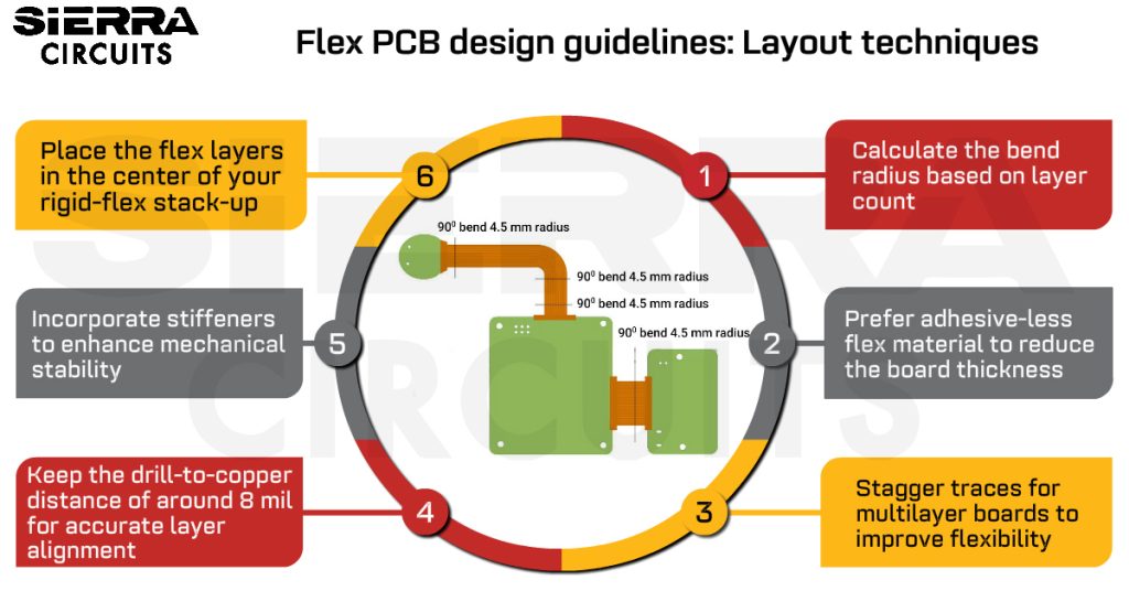
- Calculating the bend radius
- Annular ring and via specifications
- Build your flex stack-up
- Controlled impedance for flex
- The fab and drawing requirements
Download Now
Flex PCB reverse engineering challenges and solutions
The primary goal of the project was to reconstruct the flexible printed circuit to ensure solid connectivity between the LCD display and the main board.
Challenge #1: Reverse engineering the PCB to recreate Gerber files
One of the primary issues was the absence of Gerber files. These files are used to share and import graphical information such as board outlines, mechanical drawings, component footprints, and other design elements.
Without the PCB design files, extracting precise dimensions of pads, pitch, and cutouts became more complex. These details are essential for ensuring compatibility of the flex board with the other sections of the device.
Solution: Used advanced measuring instruments to assess layout properties
Our design engineers measured the required dimensions using calipers and a microscope to ensure accuracy. We also employed reticles when necessary to further enhance precision. This approach allowed us to gauge the board’s width, length, and other geometric attributes.
We communicated the measured values with the client and ensured the copper feature perfectly met their requirements.
If you’re in the same crisis wherein you don’t have the design files but have the physical board with you, partner with us to get the design files recreated and new boards manufactured.
Book a meeting with our design expert now.
Challenge#2: Gauging pad sizes, alignment, and pitch for seamless connectivity
Another critical aspect was aligning the connection pads of the flex PCB with the LCD and the main rigid circuit board. This alignment was pivotal to ensure good connectivity in the client’s device.
Solution: Recreated connection pads through inspection
We evaluated the schematic drawing of the LCD to determine the connection pad size and pitch. This analysis helped us understand the flex PCB pad size requirements on the display side. Using this data, we created footprints for the connection pads on the LCD end.
To create pads for the rigid board region, we analyzed the connection pads on the flex PCB (physical board). This involved precise measurement of pad size, pitch, and position using advanced instruments like calipers and microscopes. Based on this, we created custom footprints to ensure the connection pads’ alignment.
For more on pad design, see what is a pad in PCB design?
Sierra Circuits fabricates and assembles high quality FPCs right here in the United States. See our flex and rigid-flex PCB services to learn more.
Challenge #3: Routing 6 mil traces in a limited space
Due to the compact nature of this flex PCB, routing the connections was challenging. We had to optimize the traces to maintain signal integrity.
Solution: Optimized the trace width for effective signal transmission
Initially, we routed with a trace width of 6 mil. This choice was based on the initial assessment of the design requirements. As the project advanced, we realized that routing 6 mil traces was not feasible as it could lead to EMI.

We decided to reduce the trace width and spacing to 4 mil to accommodate all the traces within the limited space. Traces were routed in a curved path from the rigid PCB side to the LCD side.
For more on flex PCB routing, see section 3 in flex PCB design guidelines part 2: optimizing layout for manufacturing.

Key takeaways:
- Successfully reverse-engineered a flex PCB to generate Gerber files using measuring equipment like calipers, microscopes, and reticles.
- Collaborating closely with the client and utilizing the LCD schematic drawings, we recreated accurate footprints and ensured solid connectivity.
- By optimizing trace width and spacing, we maintained signal integrity while accommodating all necessary connections.
The flex PCB reverse engineering project for the LCD interface was multifaceted and required meticulous attention to detail. Despite the challenges posed by the absence of original design files, the need for precise alignment, and routing in a compact layout, our team successfully redesigned the flexible printed circuit and ensured it aligned perfectly with the client’s specifications (physical board).
Need assistance in designing your flex and rigid-flex circuit board? Post your questions on our PCB forum, SierraConnect. Our design experts will answer them.

Check out our design case studies:


Start the discussion at sierraconnect.protoexpress.com