Contents

On-demand webinar
How Good is My Shield? An Introduction to Transfer Impedance and Shielding Effectiveness
by Karen Burnham
When designing a flex circuit board, balancing structural reliability and signal integrity is paramount. In our recent project, we tackled this challenge with an innovative loose-leaf rigid-flex stack-up.
The design’s overall thickness ranges between 10 and 20 mil with a bend radius of 2 inches. Additionally, it must accommodate 253 controlled impedance traces between two connectors.
In this case study, you will learn how our flex PCB design engineers achieved the desired specs using a loose-leaf rigid-flex build-up.
Highlights:
- To achieve the desired flex thickness and bending radius, we transformed a flex design into a loose-leaf rigid-flex stack-up.
- To prevent signal overlap and maintain signal integrity, we routed 253 impedance trace signals across two leaf structures with an air gap between them.
What is a loose-leaf or air-gap rigid-flex PCB stack-up?
Design specs of this loose-leaf rigid-flex build-up
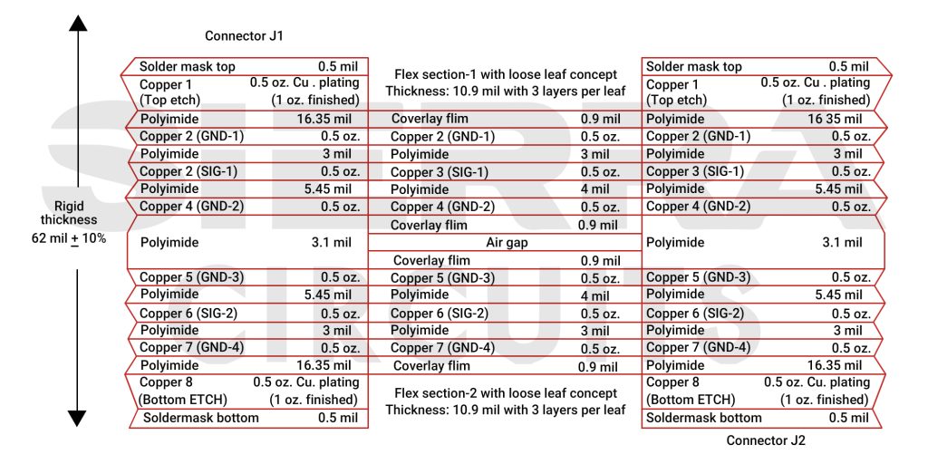
- Rigid section: 8 layers with an overall thickness of 62 ± 10 mil
- Flex section: 6 layers with an overall thickness of 21.8 mil (2 leaves with 3 layers per leaf, each of thickness 10.9 mil)
- Board dimension: 380 x 60 mm
- Copper thickness: 0.5 oz on layers 2 to 6 and 1 oz on the top and bottom layers
- Class: IPC-6013 class 2
- Connectors: 400 POS open-pin-field array connectors
- Dielectric material: N7000-2 for core and HTC 671N for prepreg
- Signals: 4.4 mil 50 Ω SE ± 10 % controlled impedance traces on both rigid and flex sections on layers 3 and 6 with min trace spacing of 4 mil
- Operating frequency: 100 MHz
- Working voltage rating: 5 V
- Maximum current rating: 100 mA
Throughout the design phase, our flex PCB designers encountered several challenges to achieve the desired thickness, flexibility, and signal integrity. In the following section, we will discuss how we overcame them to implement the loose-leaf rigid-flex stack-up successfully.
To learn how to design a cost-efficient FPC, download our design guide.
Flex PCB Design Guide
10 Chapters - 39 Pages - 45 Minute ReadWhat's Inside:
- Calculating the bend radius
- Annular ring and via specifications
- Build your flex stack-up
- Controlled impedance for flex
- The fab and drawing requirements
Download Now
Challenge #1: Achieving desired flex thickness with 253 signal lines
Since the required board thickness ranges between 10 and 20 mil, achieving the required flexibility was challenging. Additionally, both the top and bottom layers had to be ground, deviating from our usual practice of using these layers for signal routing.
This posed a significant challenge in designing a stack-up configuration accommodating 253 controlled impedance traces.
Approach 1: 10-layer stack-up with a stiffener
Initially, we proposed a 10-layer flex board with a stiffener at the connector junction. However, the overall thickness was around 27.26 mil, which reduced the bending ability.
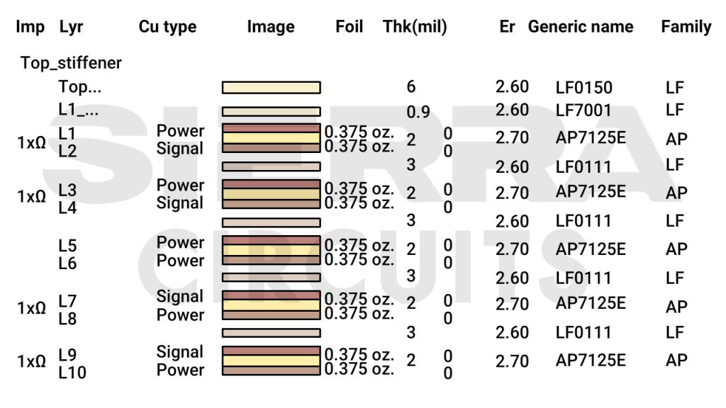
After discussing this with the manufacturing team, we realized that to achieve the desired bendability, we had to reduce the flex thickness to 10-15 mil. However, this reduction proved unfeasible.
Approach 2: 4-layer stack-up with 2 ground and 2 signal layers
Acknowledging the limitations of our previous approach, we explored an alternative stack-up. We designed a 4-layer stack-up with a sequence: ground-signal-signal-ground. To prevent signal overlap, we staggered the traces on the signal layers.
This iteration did not work, as it was difficult to fan out the connector due to space constraints.
Solution: Transforming the flex stack-up into rigid-flex
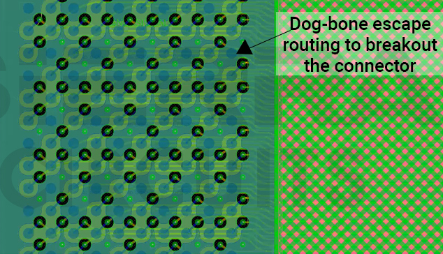
After evaluating the challenges and limitations of the previous approaches, the optimal solution involved implementing a rigid-flex configuration.
This helped us maintain the required spacing during the connector breakout.
Challenge #2: Ensuring a 4-mil clearance between flex signal layers
Despite the transition to rigid-flex, the challenge of reducing flex region thickness persisted. In addition to this, we had to maintain a 4-mil clearance between the flex signal layers.
Solution: Implementing a loose-leaf rigid-flex build-up
After having several discussions with the FPC manufacturing experts, we decided to implement a loose-leaf rigid-flex PCB stack-up. It is also called as air gap construction method in rigid-flex.
The flex section spanned layers 2 to 7, with the outer layers grounded. Implementing a two-leaf structure with an air gap between them enhanced flexibility while reducing thickness. A strategic trial-and-error approach was employed to route all signals onto two layers, optimizing signal routing and minimizing layer count.

Despite signals being distributed across different leaves with ground planes beneath them, we took precautions to ensure that signals on one leaf did not overlap with those on the other. Thus, the design achieved the desired flexibility by adopting the rigid-flex leaf structure.
Key features of loose-leaf rigid-flex stack-up:
- Flex sections are separated by an air gap, increasing the flexibility.
- The air gap between the flex sections effectively reduced the overall thickness.
- The rigid structure kept the individual flex sections stable by preventing unwanted movements.
Sierra Circuits fabricates and assembles high-quality FPCs right here in the United States. See our flex and rigid-flex PCB services to learn more.
Key takeaways:
- Implementing the air-gap construction method allowed us to route 253 controlled impedance traces without signal overlap, reducing signal integrity issues.
- Collaboration with our manufacturing team was essential in addressing the challenges of achieving the required flex thickness and bendability.
Need assistance in designing your flex and rigid-flex circuit board? Post your questions on our PCB forum, SierraConnect. Our design experts will resolve them.
Check out our series of design case studies, covering topics such as handling EMI, PCB routing issues in a medtech PCB, and integrating antennas with microcontrollers.
About Mohamed Faheemuddin : Mohamed Faheemuddin is a mechanical engineer. His passion for electronics drew him to the PCB industry. With an experience of over 3 years in the PCB industry, he specializes in developing articles for engineers and hardware designers.








Start the discussion at sierraconnect.protoexpress.com