Contents

On-demand webinar
How Good is My Shield? An Introduction to Transfer Impedance and Shielding Effectiveness
by Karen Burnham
When building PCBs for frequencies over 5 GHz and currents above 2A, trace design becomes paramount. To ensure signal integrity and reliable power delivery, optimize the trace width, spacing, and impedance of high-frequency and high-current traces.
Highlights:
When designing high-speed and high-current PCB traces:
- Implement serpentine routing, guard traces, and maintain uniform impedance to ensure signal integrity.
- Optimize trace geometry and ground planes for efficient signal propagation.
- Place decoupling capacitors near power supplies to prevent voltage drops.
- Employ thermal vias and copper pours for effective heat dissipation.
In this article, we will first cover 5 best practices for high-speed traces and move on to 5 essential guidelines for high-current traces.
At the end, you will find 5 DFM guidelines.
Watch the full webinar here: How to design high-speed and high-current PCB traces.
Key factors to consider while designing high-speed signal paths
Signal integrity becomes significant as signal speeds increase. Let’s dive into the factors you must check before designing high-speed signals for signal integrity.
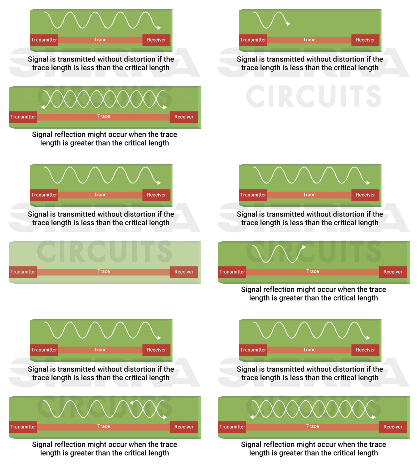
Critical length: Trace length should be less than lc
The critical length (lc) is the trace length above which a trace must be designed as a PCB transmission line with controlled impedance. If a trace is longer than the critical length, it might cause signal reflections if the impedance is inconsistent. Conversely, if the trace length is less than the critical length, the signal can be transmitted without distortion.
For analog signals, the critical length is given by:
lc = 𝛌ₘ /𝟔 = 1/ 4tpd fm
For digital signals, the critical length is given by:
lc = tr / 2tpd = (tr . V) /2
Where 𝛌ₘ = maximum wavelength of the signal
tpd = propagation delay
fₘ = maximum signal frequency
tr= rise time and V= signal speed
What is a shortline?
Shortlines refer to signal paths where the trace length is less than the critical length divided by 1.5. In these cases, signal delay and impedance mismatching are negligible.
Let’s consider a practical example to illustrate the calculation of a shortline:
- Dielectric material: FR4
- Dielectric constant: 4
- Signal rise time: 1 ns
- Signal speed: 6 inches/ns
First, calculate the critical length,
lc= tr/2 ×v = 1/2 ns ×6 inches/ns = 3 inches.
Therefore, signal traces < 3/1.5 = 2 in are considered shortlines for this design.
This means that for any trace length below this threshold, the effects of signal delay and impedance mismatching are minimal.
3 dB bandwidth: To avoid signal attenuation
3 dB bandwidth signifies the frequency range over which the transmission line can effectively transmit signals without loss. All signal frequency components propagate without distortion when the trace has a sufficient 3 dB bandwidth.
If a trace does not have adequate bandwidth, the higher-frequency components of the signal might get attenuated, leading to signal degradation and loss of integrity.
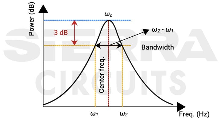
The 3 dB bandwidth is inversely related to the signal rise time. It can be calculated using the following formula:
3 dB bandwidth = 0.35/tr
Rise time (tr) is the time it takes for the signal to transition from a low to a high state (typically measured from 10% to 90% of the signal’s maximum amplitude).
For instance, if the signal rise time is 1 ns, using the above formula:
3 dB BW = 0.35/1 ns = 0.35 GHz = 350 MHz
It means the trace can effectively transmit signals with frequencies up to 350 MHz without significant attenuation.
To learn more about high-speed design, download our eBook.
High-Speed PCB Design Guide
8 Chapters - 115 Pages - 150 Minute ReadWhat's Inside:
- Explanations of signal integrity issues
- Understanding transmission lines and controlled impedance
- Selection process of high-speed PCB materials
- High-speed layout guidelines
Download Now
5 high-speed trace design techniques to ensure signal integrity
1. Implement serpentine routing for length-matching
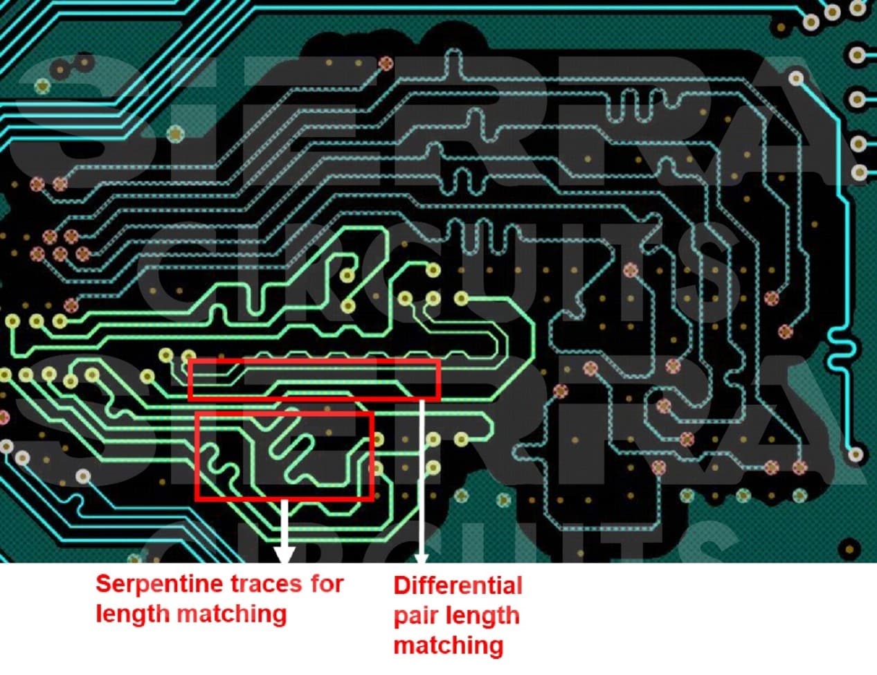
Serpentine routing and meandering are length-matching techniques used in PCB designs to ensure signals reach their destinations simultaneously. This is particularly important in high-speed and RF designs where minimizing propagation delay is critical.
This technique involves creating a series of curves or bends in a transmission line to increase its physical length without altering its electrical properties. It helps maintain the required electrical length for signals, ensuring synchronization across different traces.
Meandering incorporates similar principles, creating controlled bends to adjust the electrical length of the trace. By carefully designing these bends and maintaining uniform spacing, you can achieve the necessary length matching while preserving signal quality.
8 best tips to design serpentine traces
- Reduce the loop area created by the serpentine patterns to minimize the potential for EMI and inductive coupling.
- Ensure the spacing between adjacent trace segments is at least three times the trace width (3W) to minimize crosstalk.
- Implement smooth and controlled bends to avoid signal reflections and impedance discontinuities.
- Use simulation tools to model the electrical performance of the serpentine routing and verify that the design meets the required specifications.
- Adjust the trace width to maintain the desired impedance, especially in regions where the trace bends.
- Ensure the routing density does not exceed the PCB manufacturer’s capabilities, avoiding excessive congestion on the board.
- When designing serpentine traces, consult your manufacturer to ensure the final product meets manufacturing tolerances.
- Document the purpose and specifications of the serpentine routing in the design files to aid in review and manufacturing.
For more high-speed routing tips, see 11 best high-speed PCB routing practices.
2. Include guard traces to manage crosstalk
Guard traces create a physical barrier between critical signal traces. This separation helps minimize crosstalk, the unwanted coupling.
By surrounding sensitive signal lines with guard traces, you can suppress EM radiation from high-frequency circuits, particularly clock circuits, thereby reducing the overall EMI.
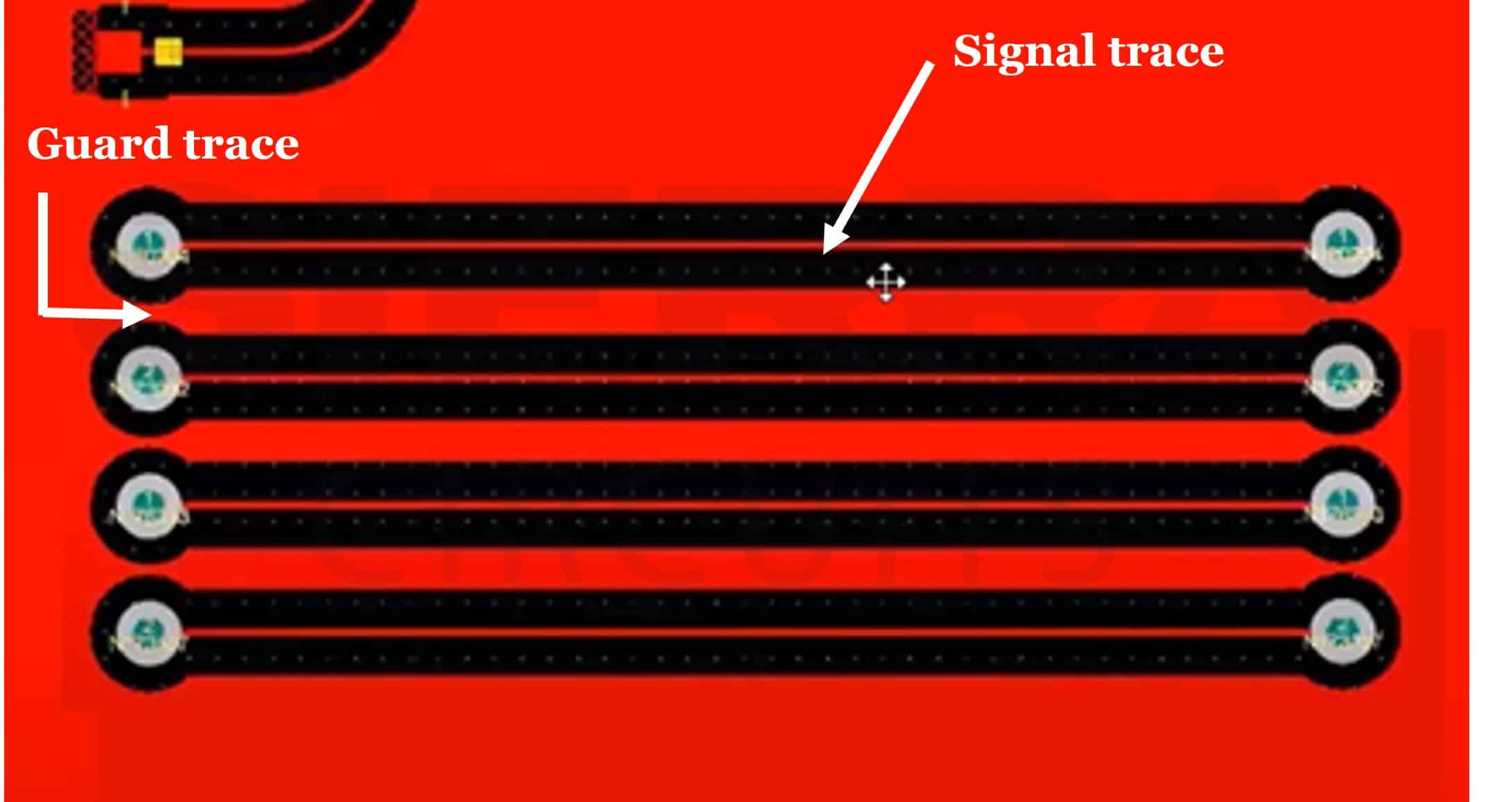
6 guidelines to implement guard traces
- Determine which signal traces are most susceptible to crosstalk and EMI.
- Place guard traces parallel to and surrounding the critical signal traces.
- Ensure they follow the same path to provide continuous shielding.
- Connect guard traces to the ground plane or a dedicated reference voltage; this provides a low-impedance path for any coupled noise.
- Keep a consistent distance of 3W to 5W between the guard traces and the critical signal traces.
- If required, place guard traces on both sides of the critical signal traces for enhanced protection.
3. Terminate traces to prevent signal reflections
Signal reflections occur when there is a mismatch between the impedance of the transmission line and the components connected to it. To prevent these signal reflections, you need to design your trace terminations carefully.
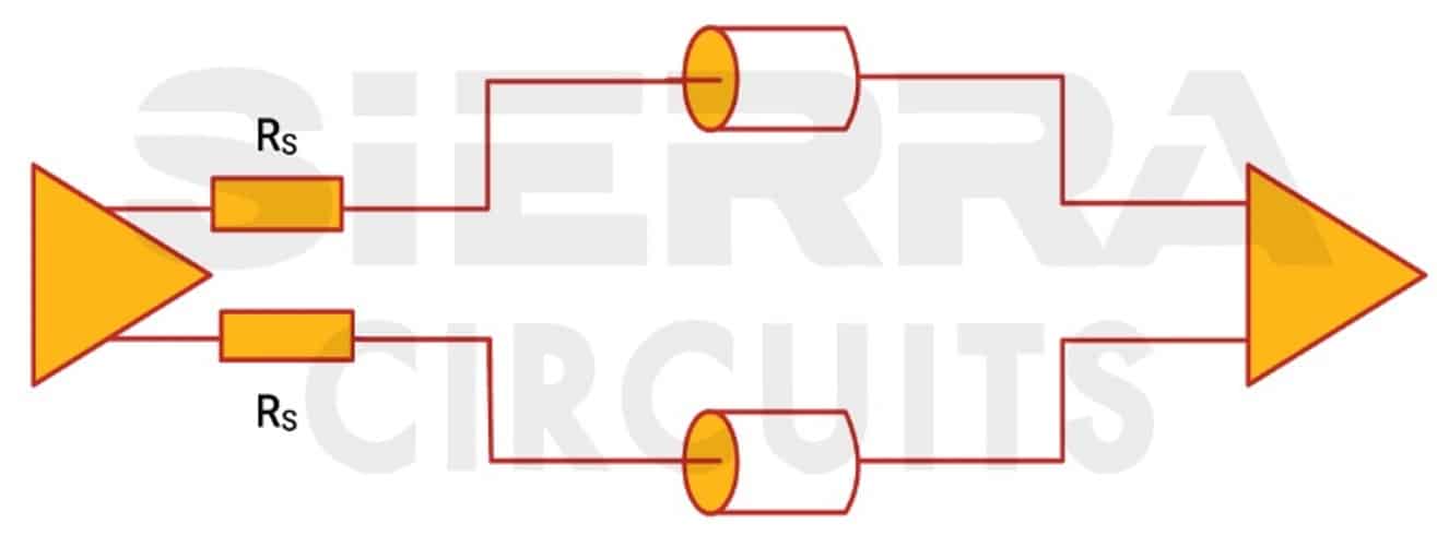
Series trace termination
In series trace termination, place a terminating resistor between the driver and the transmission line. This resistor should be as close to the driver as possible to ensure proper signal damping. The purpose of the series resistor is to create an impedance match between the driver and the transmission line.
You must carefully select the value of the series resistor so that the combined impedance of the driver and resistor matches the trace impedance.
For example, if the driver impedance is 23Ω and the trace impedance is 50Ω, you would use a series resistor of (50 – 23) = 27Ω.

For differential pairs, where two traces carry complementary signals, you should place a series resistor in each line. This helps to minimize any mismatch in the differential impedance and reduces signal reflections.
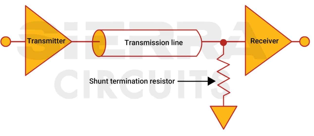
Parallel/shunt trace termination
Parallel termination involves placing a shunt resistor at the end of the transmission line, close to the receiver. This termination technique helps absorb the reflected signals at the receiver end, minimizing the chances of signal reflections and improving signal integrity. Shunt termination requires more power than series termination and often introduces additional stubs in the designs.
This shunt resistor can be a pull-up resistor or a pull-down resistor. Pull-up resistors must be connected to the power supply, whereas pull-down resistors are grounded for the reference potential.
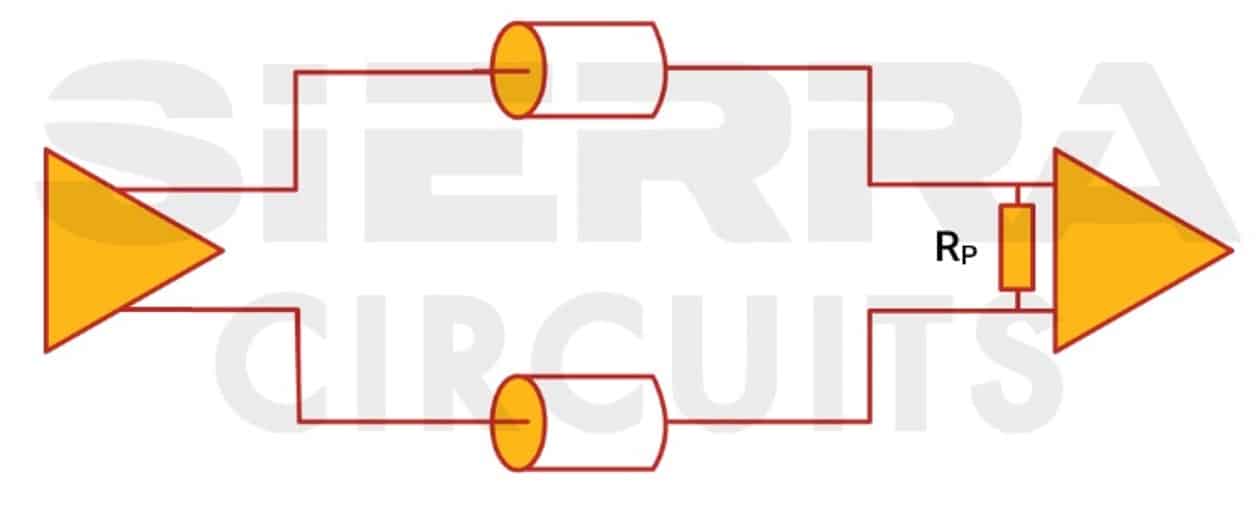
For differential routing, the termination resistors are placed in parallel across the two lines.
To learn more termination techniques, see 5 PCB trace termination techniques to reduce signal reflections.
4. Optimize the trace geometry to ensure consistent impedance
To design transmission lines with controlled impedance, stick to the following guidelines:
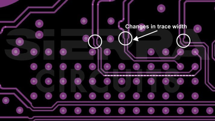
1. Maintain a consistent trace width along your transmission lines. Sudden changes in trace width might cause impedance mismatches, leading to signal reflections. While changing the trace width, you need to taper the transition gradually to minimize the risks of signal degradation.
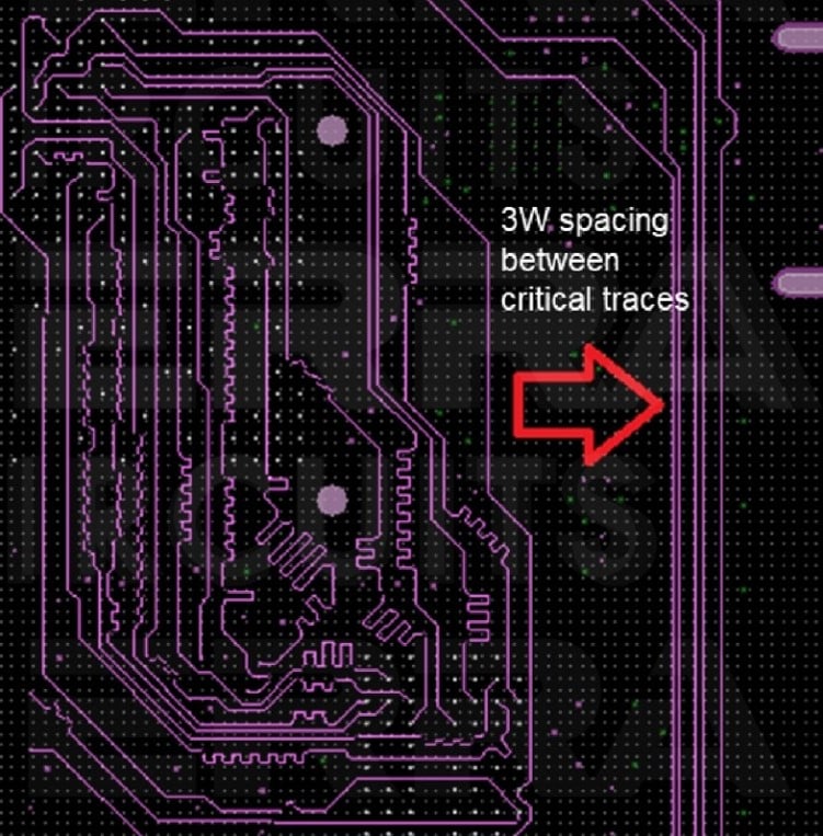
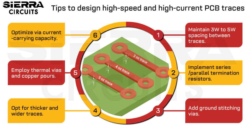
2. Maintain 3W to 5W spacing between traces to minimize crosstalk and ensure consistent impedance.
3. Avoid running RF traces parallel to other signal traces to prevent coupling. Running traces in parallel increases electromagnetic interference, particularly at high frequencies. To minimize these issues, route RF traces perpendicularly to reduce coupling effects.
4. Use daisy chain routing instead of multi-point branches to reduce undesired stubs. Daisy chain routing connects components in a series, minimizing the formation of stubs that can cause signal reflections and distortions. Multi-point branches, on the other hand, create more stubs that act as impedance mismatches, causing signal loss and interference.

5. Another important consideration is matching the trace impedance to the impedance of the connectors used in the circuit. The mismatched impedance between the trace and connectors can lead to significant signal degradation.

At Sierra Circuits, we add impedance test coupons to each panel and validate the impedance during fabrication. These test coupons replicate the trace structure and layer stack-up of the actual PCB. See controlled impedance capabilities to learn more.
5. Never split ground planes
Proper grounding is essential for high-speed signal lines to minimize electromagnetic interference and reduce noise. It provides a stable reference point, preventing signal distortion and data errors.
6 best grounding practices to ensure signal integrity and minimize EMI
- Keep the signal return path short to minimize parasitic capacitance and inductance. Avoid creating large loop areas, as they can act as antennas and pick up unwanted noise.
- When a signal changes from one reference plane to another, include transition vias close to the signal vias. This ensures a continuous return path for the signal and minimizes the chance of reflections.
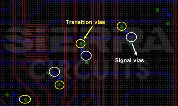
Transition vias connect the ground plane on different PCB layers, effectively reducing the loop inductance in the ground path. - High-speed or critical signals should have dedicated reference planes to ensure stable operation and reduce the likelihood of noise coupling into the signal.
- A continuous, unbroken ground plane offers noise reduction and signal integrity. Hence, never split ground planes, as this can create noise-inducing voltage differentials between different sections of the PCB.
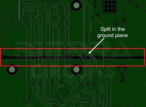
A layout image showing splits in the ground plane. This causes impedance discontinuity. - To make the most of unused space, use copper pours connected to the ground plane. This provides additional shielding and helps with heat dissipation. The spacing between a high-speed/RF trace and ground pours should be 1.5 to 2 times the trace width. Ensure ground pours do not create isolated ground islands, which can act as unintended antennas.
- Implement via stitching along the ground plane edges or RF traces to provide multiple low-impedance return paths. Via stitching creates multiple electrical connection points between layers, reducing ground impedance and enhancing shielding for sensitive high-speed and high-current PCB traces. These vias also help contain electromagnetic interference, improving overall signal integrity.
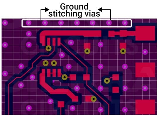
The via stitching gap should be between λ/20 and λ/10; λ is the operating signal wavelength. This guideline for via spacing ensures optimal isolation and minimizes unwanted radiation at high frequencies.
To learn how to build an efficient PCB stack-up, download our design guide.
![]()
PCB Stack-Up Design Guide
12 Chapters - 55 Pages - 60 Minute Read
What's Inside:
Download Now
5 high-current trace design techniques to ensure power integrity
Ensuring power integrity in high-current PCB designs requires careful attention to trace width, copper thickness, and temperature rise. Power integrity issues can lead to voltage drops, noise, and even permanent damage to the PCB components.
1. Calculate the trace current-carrying capacity
To calculate the current-carrying capacity of a trace, you can use the formula from IPC-2221, which considers factors like temperature rise, cross-sectional area, and conductor thickness.
I = (K) (𝝙T𝜷1) (A𝜷2)
Where,
I is the current in amperes
𝝙T is the temperature change with respect to the ambient temperature in °C
A is the cross-sectional area in mil
K is the correction factor, which equals 0.024 for internal conductors and 0.048 for external conductors
𝛽1 and 𝛽2 are 0.44 and 0.75, respectively
This formula is useful for determining whether a trace can handle the required current without excessive heating.
You can use Sierra Circuits’ Trace Width, Current Capacity, and Temperature Rise Calculator to simplify these calculations.
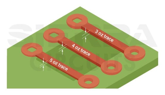
2. Use wider traces
When designing high-current traces, the primary factors you need to consider are the target current, the maximum allowable temperature rise, copper thickness, and the trace’s resistance.
To handle higher currents, wider traces are recommended, as they have higher current-carrying capacity (ampacity) and lower resistance.
Also, use shorter traces, since shorter traces have lower resistance, which reduces power loss and heat generation.
3. Place the thermal vias near the hotspots
Managing heat is crucial for maintaining circuit reliability in high-current PCB designs. Overheating can lead to premature failure of components or even damage the PCB itself.
3 ways to reduce heat in high-current traces:
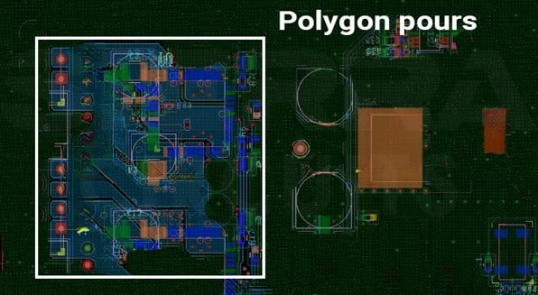
- Use copper pours instead of narrow traces for high-current paths. These large areas of copper spread the heat more efficiently and reduce the risk of overheating.
In one of our recent medtech projects, routing high-current traces between the stepper motor connector and the driver increases the risk of overheating due to the confined space for the current flow.
Our PCB layout engineers opted for polygons instead of traces to overcome this routing issue. We established a seamless connection between the stepper motor connector and the driver by utilizing polygon pours. This provided ample room for high currents to flow without the risk of overheating.
For more on the techniques we implemented to avoid EMI in this medtech circuit board, see Case Study: Resolving EMI and PCB Routing Issues in a Medical Optical Scanner.
2. Choose PCB materials with high thermal conductivity, such as ceramic-filled PTFE substrates.
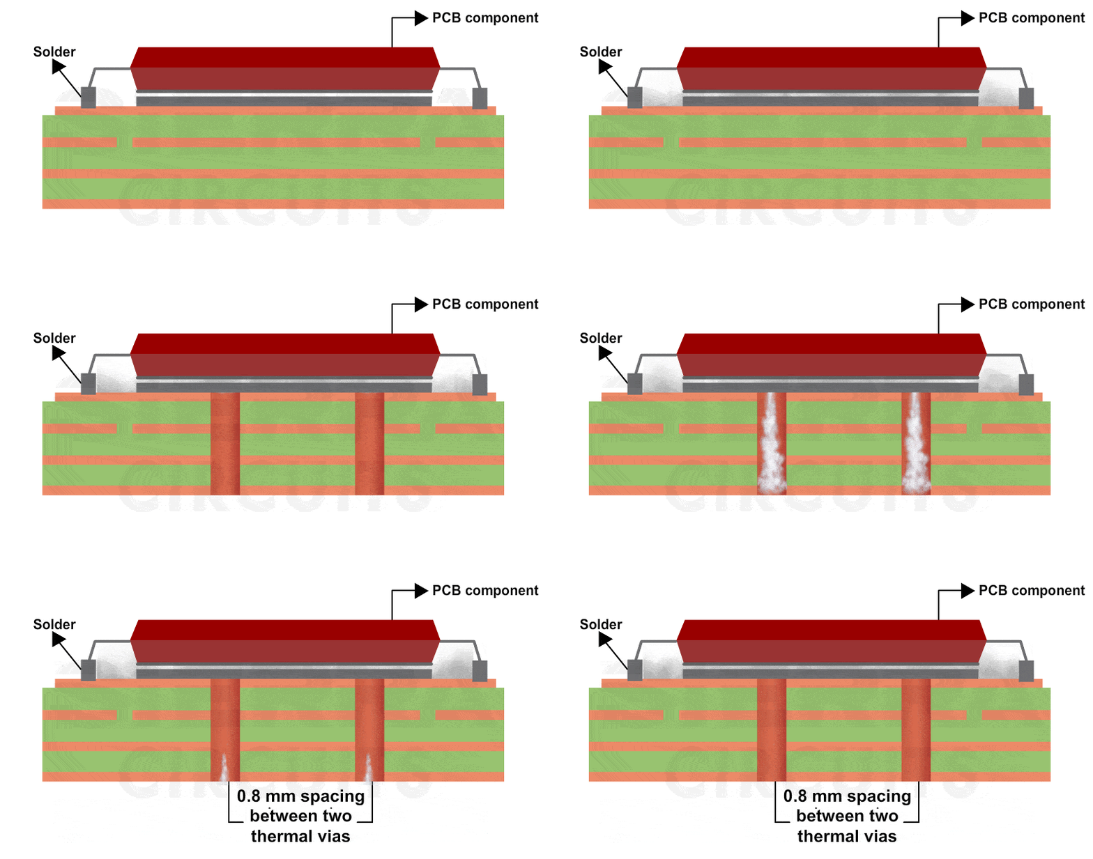
3. Place the thermal vias near the heat source to lower the thermal resistance and increase the heat dissipation rate. This layout allows heat to quickly transfer from the source to the other layers, reducing localized hotspots.
Include thermal vias directly under the thermal solder pads for circuit boards with more than 0.7 mm (28 mil) thickness. Choose a 0.3 mm via diameter and 0.8 mm via-to-via spacing. This balances mechanical stability and thermal performance without compromising board integrity.
For more PCB heat management tips, see 12 PCB thermal management techniques to reduce heating.
4. Place decoupling capacitors near the power supply
In high-power circuits, sudden surges in current demand can cause voltage dips, leading to instability in the system. Decoupling capacitors act as local reservoirs of charge that supply this additional current when needed, helping to maintain a stable power supply.
Use multiple low-inductance decoupling capacitors of the same value. To ensure maximum efficiency, place the decoupling capacitors as close as possible to the power and ground pins of the IC.
This minimizes the loop inductance and improves the capacitor’s effectiveness in supplying instantaneous current. For high-power applications, incorporate low ESR (equivalent series resistance) ceramic capacitors with 0.1 µF and 0.01 µF capacitance.
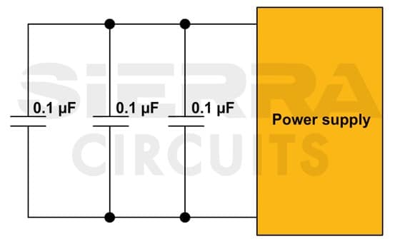
Mount the decoupling capacitors on the same layer as the components to reduce the parasitic inductance of vias, enhancing their effectiveness at high frequencies. This proximity minimizes impedance in the power supply path, providing stable power to the components. Additionally, position decoupling capacitors parallel to the high-speed and high-current PCB traces to maintain a direct, low-impedance path to the ground.
Read how to create a schematic for high-speed designs in KiCad for PCB prelayout design tips.
5. Optimize via current-carrying capacity
If vias are designed without considering the current rating, they can overheat. This overheating risks damaging adjacent traces, weakening solder joints, and even causing board delamination.
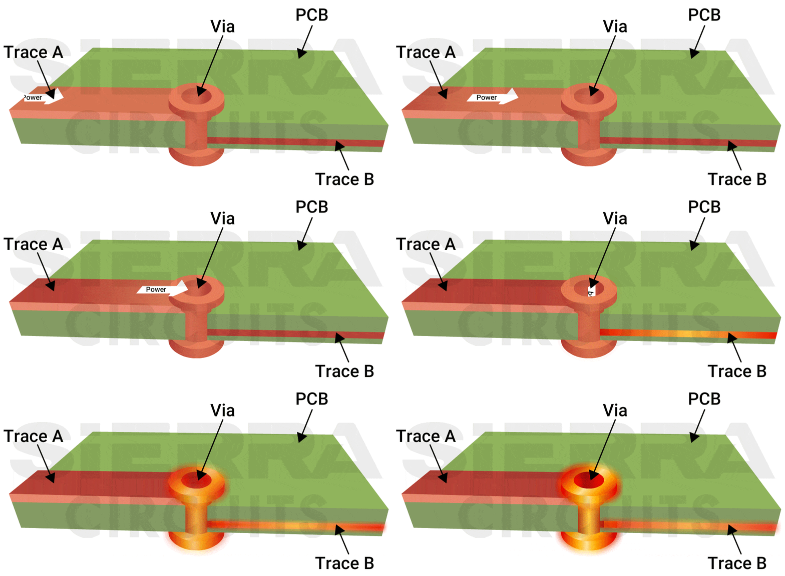
To ensure vias are designed with optimum current-carrying capacity:
Increase the number of vias connecting the power path to enhance the total cross-sectional area for current flow and reduce the voltage drop.
Adding more vias along the power path increases the effective cross-sectional area, which reduces the current density through each via. This distribution also lowers resistive losses, minimizes voltage drop, and prevents individual vias from overheating. A greater number of vias also supports more stable and reliable power delivery to high-current components.
Arrange vias close together to increase the conductivity, reducing resistive losses and allowing higher current flow. Grouping vias closely provides a compact, low-resistance path for current flow, enhancing conductivity and reducing overall resistive losses.
In addition, tight via clusters also help manage power distribution effectively, especially in high-current applications.
Use through-hole vias rather than blind or buried vias for high-current traces. Through-hole vias provide a continuous conductive path across all board layers, ideal for handling high currents.
Blind or buried vias, while useful in compact designs, can have higher resistance and limited thermal paths, making them less suitable for high-current applications.
To learn more about via current capacity, see how to design via for current carrying capacity.
5 best DFM guidelines for high-speed and high-current PCB traces
1. Stick to the manufacturer’s minimum/maximum line width capabilities
Using trace widths outside the manufacturer’s specified range can lead to incomplete etching or over-etching, which may cause open circuits or inconsistent signal paths. Staying within these capabilities ensures reliable trace formation, minimizes production errors, and enhances the board’s overall quality.
2. Maintain sufficient trace spacing based on the start copper thickness
Trace spacing must be based on the starting copper thickness, as thicker copper layers require more spacing to prevent electrical shorts. Proper spacing also reduces crosstalk by minimizing electromagnetic coupling between adjacent traces. By following recommended line spacing, you maintain signal integrity and prevent interference across high-speed and high-current PCB traces.
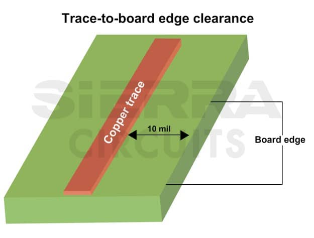
3. Provide at least 7 mil trace-to-board edge spacing for outer layers and 10 mil for inner layers
Ensuring a sufficient gap between traces and the board edge reduces EMI. A 7 mil spacing on the outer and 10 mil on the inner layers also protects traces against mechanical stresses, reducing the risk of short circuits due to exposed copper near the edge.
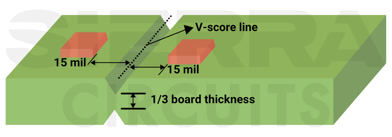
4. Ensure at least 15 mil clearance between the copper feature and the v-score line
This clearance prevents the v-scoring process from cutting into copper features, which could cause electrical shorts or weaken the mechanical structure of the high-speed and high-current PCB traces.
5. Have a minimum of 8 mil drill-to-copper clearance to avoid short circuits
An 8 mil drill-to-copper clearance ensures drilled holes don’t accidentally contact copper traces, which could result in short circuits or signal integrity issues. This spacing also compensates for potential drill wander, preserving electrical isolation between the hole and nearby conductive elements.
See our interview to learn more about the benefits of HSD apps by tim wang lee.
Key takeaways:
- Keep trace lengths as short as possible.
- Add ground stitching vias.
- Maintain 3W to 5W spacing between traces.
- Provide a continuous ground plane for high-speed and high-current PCB traces.
- Implement series/parallel termination near the source end to ensure controlled impedance.
- Opt for thicker and wider traces to increase trace current carrying capacity.
- Refer to the manufacturer’s guidelines for trace width/clearance based on copper weight.
- Employ thermal relief techniques, such as thermal vias and copper pours.
By understanding the principles of signal integrity, power integrity, and thermal management, you can effectively design high-speed and high-current PCB traces that meet the stringent requirements of modern electronic systems.
Do you need assistance in planning the layout of your upcoming PCB project? Connect with us on our forum, SierraConnect.
About Poulomi Ghosh : Poulomi is a microwave engineer specializing in EMI, EMC, RF, and high-speed electronics. As a senior technical writer at Sierra Circuits, she creates advanced engineering articles and webinars for hardware engineers and PCB designers.







What are the best practices for designing high-current power planes to minimize voltage drops and ensure uniform current distribution?
Hi Michael,
Here are some best practices for designing high-current power planes:
What are the challenges and solutions for designing high-speed, high-current PCBs for automotive applications?
Hi John,
Automotive applications have stringent requirements for reliability, EMC, and thermal management. Here are some challenges and solutions: