


Contents

On-demand webinar
How Good is My Shield? An Introduction to Transfer Impedance and Shielding Effectiveness
by Karen Burnham
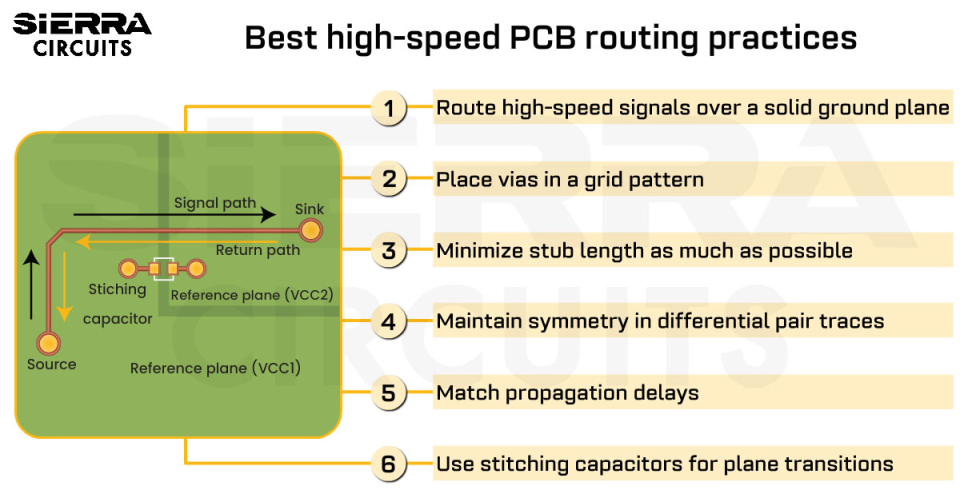
When routing high-speed PCBs, always place a solid ground plane beneath signal traces to maintain signal integrity and reduce EMI. Arrange vias in a grid pattern to prevent plane voids and hot spots that can disrupt current flow. Maintain symmetry and consistent spacing between differential pair traces to preserve impedance balance and minimize crosstalk.
At gigahertz (GHz) frequencies, even small layout errors can cause reflections and timing mismatches. Hence, PCB designers and layout engineers must follow proven high-speed routing practices to ensure clean, interference-free signal propagation.
In this article, you’ll learn the 10 best high-frequency circuit board routing practices to maintain signal quality, reduce crosstalk, and ensure consistent impedance.
Highlights:
- Maintain consistent impedance and provide controlled return paths to ensure stable high-speed signal performance.
- Use a solid ground plane to create a low-impedance return path, reduce EMI, and stabilize high-frequency signals.
- Optimize via placement, trace spacing, and minimize stub length to maintain uniform impedance and minimize crosstalk or reflections.
- Preserve symmetry and match propagation delay in differential pairs to support high-speed interfaces such as USB, HDMI, and PCIe.
- Avoid routing over split or voided planes; if unavoidable, place stitching vias or capacitors near the transition points to maintain signal continuity.
- Keep traces at least 10-15 mil away from board or plane edges to prevent impedance variation and EMI leakage.
- Plan your layer stack-up and routing topology early, as these directly influence manufacturability, signal timing, and thermal performance.
1. Route high-speed signals over a solid ground plane
A solid ground plane provides a low-impedance return path, minimizes EMI, and stabilizes signal impedance. Without it, return currents spread unpredictably, increasing noise and timing errors.
Let’s see how this tip can be effectively implemented in different PCB design scenarios.
Scenario 1: Multilayer stack-up
- Dedicate an internal layer for ground (preferably inner layer 1). This gives high-speed traces on the outer layers a solid reference plane right underneath them. It also helps you maintain consistent impedance and reduce current loop size.
- Place high-speed components on the top layer, which is adjacent to the ground plane.
- Reserve the other external layer for less critical components.
- Use the second inner layer (inner layer 2) for the power plane. This ensures efficient decoupling.

Scenario 2: 2-layer build-up
- Route signal and power traces on the top layer and dedicate the bottom layer to a solid ground plane.
- If you’d like to route traces on both layers, the ground plane becomes fragmented, leading to inconsistent return paths. To avoid this, add ground pours on both sides and connect them with stitching vias to maintain continuity.

Do not split the ground plane, as it forces high-frequency return currents to take long, unpredictable paths around the gap, increasing noise and EMI.
For better results, isolate analog and digital sections functionally by grouping and routing components separately.
6 tips for designing efficient ground planes
- Have a continuous ground plane with no breaks to avoid impedance discontinuities.
- Include a dedicated ground plane for every high-speed or RF signal layer.
- Implement via stitching along ground plane edges or near RF traces to provide multiple low-impedance return paths.
- The via stitching pitch should be between λ/20 and λ/10, where λ is the operating signal wavelength.
- Use ground pours on both outer layers in RF and high-speed designs to help suppress EMI and crosstalk.
- Maintain a spacing of 1.5 to 2 times the trace width between high-speed traces and adjacent ground pours.
- Ensure ground pours are properly connected to the main ground network. Isolated ground regions can act as unintended antennas and radiate noise.
Download our High-Speed PCB Design Guide for more layout guidelines.

High-Speed PCB Design Guide
8 Chapters - 115 Pages - 150 Minute ReadWhat's Inside:
- Explanations of signal integrity issues
- Understanding transmission lines and controlled impedance
- Selection process of high-speed PCB materials
- High-speed layout guidelines
Download Now
2. Place vias in a grid pattern to avoid plane voids and hot spots
Improper via placement can disrupt current flow and create localized high-current density areas, known as hot spots. These regions increase impedance, generate heat, and impact power integrity.
To maintain even current distribution, arrange vias in a uniform grid pattern rather than clustering them. A consistent via matrix allows current to flow continuously across the ground and power planes, minimizing voids and thermal buildup.

Maintain at least 15 mil spacing between vias wherever possible (smaller spacing may be acceptable in dense BGA regions).
When routing high-power signals or thermally sensitive components, use an array of thermal vias under the part’s thermal pad. These vias transfer heat efficiently into the internal ground plane.
Closely spaced vias can cause overlapping antipads, creating large gaps in the copper plane that disrupt return paths and impedance continuity.

Download our PCB Via Design Guide to learn how to create reliable plated holes.

PCB Via Design Guide
7 Chapters - 90 Pages - 70 Minute ReadWhat's Inside:
- Guidelines for choosing the right via for your application
- Design rules for advanced via structures
- DFM tips to avoid manufacturing errors
- Signal integrity considerations for high-speed designs
- Testing and inspection methods for via reliability
- Fab notes
Download Now
3. Increase the spacing between the signals outside the bottleneck regions to evade crosstalk
When high-speed signals travel close together, the changing electromagnetic fields of one trace (aggressor) can induce voltage/current onto an adjacent trace (victim), leading to crosstalk. The simplest and most effective way to minimize crosstalk is by increasing the spacing between adjacent traces. The magnitude of the interaction can be reduced by the square of the distance.

In dense regions (bottlenecks), you may have limited room to have enough clearance. In such cases, maintain the minimum allowable spacing in the bottleneck regions, but increase spacing immediately after (as shown in the image below). This helps field coupling decay more rapidly.

4. Minimize stub length as much as possible
A stub is an unintended branch or leftover segment of a trace or via that doesn’t follow the main signal path. The longer the stub, the more it can distort or reflect the signal.
At high frequencies, even small stubs act as resonant open circuits, reflecting signals back toward the source. These reflections cause signal degradation, timing errors, and in severe cases, loss of eye diagram integrity.
As data rates climb above 3 Gbps, via stubs become a critical source of losses in PCB transmission lines.
3 design tips to prevent signal reflections caused by stubs
- Keep the stub length shorter than one-quarter of the switching speed of the driver (the lumped distance). If possible, reduce stub length even further, ideally less than one-tenth of the wavelength for better signal integrity.
- Use via-in-pad or back-drilling techniques to eliminate stubs.
- Avoid T-branch connections (especially in differential pairs) and implement daisy-chain routing. However, keep in mind that daisy-chain topologies are best suited for designs where tight signal timing isn’t a critical concern.
- Pull-up or pull-down resistors on high-speed signals are common sources of stubs. If such resistors are necessary, route the signals as a daisy chain, as illustrated below.


5. Maintain symmetry in differential pair traces
Differential pairs carry complementary single-ended signals that rely on precise timing and phase balance. Any mismatch in length, spacing, or geometry between the two traces leads to skew, mode conversion, and loss of noise immunity.
Maintaining symmetry ensures both lines experience the same impedance environment and delay, preserving signal integrity at high speeds.
6 differential pair routing guidelines for maintaining uniform impedance
- Make sure the trace geometry is within your manufacturer’s tolerance, typically ±5 mil for high-speed designs.

- Maintain uniform clearance between the traces along the entire length (even around bends or vias) and ensure a continuous reference plane beneath traces.
- Route both traces on the same layer whenever possible to avoid differential impedance variation. When routing across layers, use vias of equal length and number in both traces to preserve timing and impedance.

-
- For high-speed interfaces like USB 3.0 or PCIe, even a 25–50 ps skew can degrade performance. Keep differential impedance tightly controlled, typically 90 Ω ± 10%.
- If diff. pairs require serial coupling capacitors (AC coupling), place them symmetrically as shown in the image below. The capacitors create impedance discontinuities, so placing them symmetrically will reduce the risks of signal skew. Smaller component packages (like 0402) are preferable as they introduce less parasitic capacitance and inductance.

-
- If you’re having vias on diff. pairs, place them symmetrically as shown below. Each trace in the differential pair should have the same number of vias in the same relative positions. This ensures uniform signal length.

Sierra Circuits can fabricate high-speed PCBs with an impedance tolerance of ±5%. Visit our controlled impedance capabilities to learn more.
6. Match propagation delays to ensure timing alignment
In high-speed designs, signals should travel at identical speeds across all traces. Differences in trace length, dielectric constant, or routing layer can cause variations in signal speed, leading to timing mismatches (skew).
Let’s see how propagation delay matching can be implemented in various high-speed design situations.
Scenario 1: Parallel data or address bus
All signals must arrive at the receiver within a specific time window for the system to read the data correctly.
Keep the propagation delay differences (timing skew) within the limits defined by your interface datasheet.
Use length-matching techniques to align timing. But remember, the goal is to achieve timing alignment, not necessarily identical trace lengths.
Scenario 2: Differential pair routing
In differential signals (like USB, LVDS, or HDMI), both traces must switch simultaneously to maintain balanced coupling.
Both traces must have the same propagation delay to switch simultaneously and maintain balanced coupling. If there’s any skew, you can fix it using serpentine (meander) tuning, as shown in the image below.

Use serpentine (accordion) routing to fine-tune shorter traces to match longer ones. This correction should be applied as close as possible to the point of mismatch (e.g., near a via or component) as shown below. The mismatch occurs on the left set of vias, so add the serpentine on the left.

Bends can also cause inconsistencies if the trace on the inner bend is smaller than the outer trace. In such cases, compensate close to the bend area as shown below.

Route both traces on the same layer to ensure equal signal speeds and a consistent dielectric constant. If a differential pair signal changes from one layer to another using vias and has a bend, each segment of the pair needs to be matched individually.
In the image below, the vias separate the differential pair into two segments.

Scenario 3: Component pad and breakout regions
Some EDA tools also consider the trace length inside a pad as its total length. The image shown below depicts two layouts that are similar from an electrical point of view.

On the left, the traces inside the capacitor pads do not have an equal length. Even though the signals do not use internal traces, some CAD tools consider this as part of the length calculation and display a length difference between the positive and negative signals. To minimize this, ensure that the pad entry is equal for both signals.
Always prefer a symmetrical breakout, as shown in the image below.

Small loops can be included for the shorter trace instead of serpentine traces if there is enough space between pads. This is generally preferred over a serpentine trace.

Physical trace length vs. electrical trace length
Designers often focus on the physical aspect of the trace length and overlook the electrical aspect. Consider both to manage signal skew effectively.
| Physical trace length | Electrical trace length | |
|---|---|---|
| What it represents | The actual measured trace length. Typically expressed in mil or mm. | The effective signal propagation delay along a trace, measured in time (ps). |
| How to match |
|
|
7. Do not route a signal over a split plane
Routing high-speed or sensitive signals across split planes breaks the return current path, creating loop discontinuities and impedance mismatches. This can lead to EMI radiation, signal distortion, and even ground bounce in mixed-signal or power-dense designs.
Always have a solid ground plane beneath the signal, as shown below.

Low-speed signals follow the path of lowest resistance (the shortest physical path). At high speeds, the return current follows the path of lowest impedance, which is typically directly beneath the signal trace on the adjacent reference plane, as illustrated below.

8. Use stitching capacitors for plane transitions
If routing a signal trace across a split or slot is necessary, place stitching capacitors at the transition point, as shown in the image below.

The stitching capacitor allows the return current to flow smoothly from one plane to the other, minimizing the loop area.
Place the capacitor as close as possible to the signal transition point to keep the forward and return paths tightly coupled. Typical stitching capacitor values range from 10 nF to 100 nF.
Let’s see how stitching capacitors can be effectively implemented in different high-speed routing scenarios.
Scenario 1: Routing over a split plane or slot
In general, avoid plane obstructions (slots) whenever possible. If routing over them is unavoidable, use stitching capacitors as illustrated below. This ensures a continuous current path.

Scenario 2: Routing a signal over a power plane
When a high-speed signal is routed over a power plane, that plane acts as the signal’s reference instead of the ground plane. The return current will therefore flow along the power plane.
Since most source and sink circuits are referenced to ground, this difference in reference can create return path discontinuities. To minimize them, place stitching capacitors near the source and sink to provide a low-impedance AC path between the power and ground planes.
Use stitching capacitors when routing over a power plane in high-speed PCBs.

Scenario 3: Layer transition with a different reference plane
When a differential signal changes layers, the reference plane beneath it may also change. To maintain a continuous return path, place stitching vias symmetrically close to the signal vias at the layer transition, as illustrated below.
These vias allow the return current to shift smoothly between reference planes without increasing loop area or causing EMI.

Scenario 4: Transition between ground and power reference planes
When a signal transitions between layers with different reference planes (for example, from a ground plane to a power plane), place stitching capacitors near the layer transition point. These capacitors provide a local AC return path, allowing the return current to flow smoothly between the two planes and minimizing EMI.
These capacitors provide a local AC return path, allowing the return current to flow smoothly between the two planes and minimizing EMI.

If the reference planes on both layers share the same net (for example, continuous ground), stitching vias alone are sufficient, and capacitors are not necessary.
Need help in designing reliable high-speed PCBs? Our engineering team can help you with schematics, stack-up design, layout design, and DFM analysis.
You can book a meeting with our experts or call us at +1 (800) 763-7503.

9. Add dedicated ground vias close to the source and sink of the signal
Each signal via represents a discontinuity in the return path. Without a nearby ground via, the return current must take a long detour to reach the new reference plane.
In the image shown below, the left one is considered to be a bad design. Since there is only one ground via near the source, the return current is forced to flow along the top-layer ground trace instead of the internal ground plane.

Hence, place dedicated ground vias immediately adjacent to the signal via at both the source and sink of the signal. This ensures the high-frequency return current has a direct, low-inductance path to transition to the internal ground plane.
10. Keep high-speed traces away from board and plane edges
Routing traces too close to the edge of the PCB or the edge of a reference plane can distort the electromagnetic field and change the signal’s impedance. To avoid this, keep your traces at least 10–15 mil away from the board or plane edge. This spacing helps reduce fringing fields and prevents unwanted EMI leakage.

Achieving a good high-speed PCB routing depends on balancing signal performance with manufacturability. Every trace and via impacts signal quality, so planning the layout carefully from the start is essential. Close collaboration with your fabricator and following proven routing practices helps maintain impedance control, minimize EMI, and ensure reliable performance at high frequencies.
About the technical reviewer:
Dilip Kumar is the Senior Design Manager at Sierra Circuits with over a decade of experience in developing high-speed and HDI PCB designs featuring fine-pitch BGAs. He is proficient in Altium Designer, Cadence Allegro, Eagle PCB, KiCAD, and AutoCAD.
Leading a team of skilled PCB designers and layout engineers, he oversees projects from concept to production, ensuring precision and manufacturability at every stage. Dilip consistently delivers innovative, high-quality designs that meet demanding engineering and business objectives.
Have queries regarding designing high-speed layouts? Post them on our community, SierraConnect. Our design experts will answer them.

About Rahul Shashikanth : Rahul Shashikanth is an electronics and communication engineer with over 8 years of experience in publishing technical articles on PCB design, manufacturing, and assembly. He is currently the content marketing manager at Sierra Circuits.


I’m currently working on a high-speed PCB design and have some questions about transmission line effects. From my understanding, when we talk about “transmission line” effects, we refer to issues like crosstalk, reflections, and ringing. These effects don’t usually appear at low frequencies where the PCB trace behaves more like an ideal transmission medium, similar to how we expect a wire to behave based on early school lessons.
I also understand that the 50-ohm value isn’t related to the line resistance, which is typically very small and less than 1 ohm. Instead, this value comes from the ratio of the inductance (L) and capacitance (C) on the line. Adjusting the trace height above the ground plane (affecting C) or changing the trace width (affecting L) can change the impedance of the line.
Since the reactance of L and C depends on the signal frequency, I have a few questions:
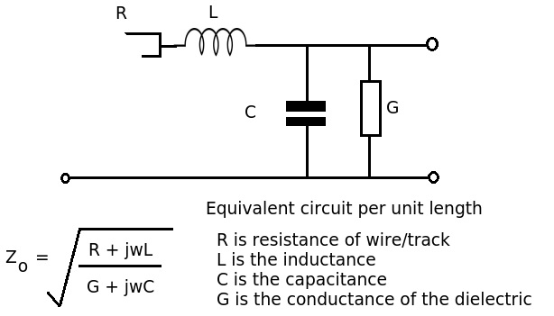
First, let’s have a look at the formula and equivalent circuit for a transmission line:
1. Impedance vs. Reactance
Reactance describes the opposition to changes in current or voltage for individual components like inductors and capacitors. A transmission line, however, incorporates resistance (R), inductance (L), and capacitance (C), making impedance the appropriate term. Impedance is defined as the ratio of the voltage phasor to the current phasor in a transmission line, encompassing all these elements.
2. Why 50Ω?
The 50Ω impedance arises from the ratio of inductance to capacitance per unit length of the transmission line. When R is much less than jωL and G is close to zero, these values become negligible, simplifying the expression to the square root of L/C, making it frequency-independent.
3. Deviating from Standard Impedance
Technically, you can choose any impedance, such as 100Ω or 167Ω, but it’s generally advisable to stick to standard values like 50Ω. This is because finding compatible components, such as connectors for non-standard impedances, can be challenging. Additionally, there are extensive resources and guidelines available for designing transmission lines on PCBs. As a side note, the impedance of free space is 376.73031… ohms, which is an interesting fundamental constant of our universe.
4. When Actual Resistance Matters
At low frequencies, the resistance (R) of the transmission line may become significant as the inductive reactance (jωL) is small. At very high frequencies, dielectric losses can also become a concern, affecting the performance of the transmission line.
A transmission line inherently possesses distributed inductance and capacitance throughout its length, which can be conceptualized as countless small inductors and capacitors arrayed along the line, as shown below:

Each inductor slows down the rate at which its corresponding capacitor can charge. As we continue to subdivide the transmission line into smaller and smaller segments, the inductors and capacitors become proportionately smaller as well. But does this subdivision affect the line’s behavior? Not really. We can slice the transmission line into any number of segments—from just a few to an infinite number—making the inductors and capacitors arbitrarily small in the process.
The critical insight here is that the absolute values of these inductors and capacitors are not what dictate the line’s properties. What truly matters is the ratio of inductance to capacitance, a value that remains constant regardless of how much we divide the line. Since the characteristic impedance of the transmission line is determined by this ratio, it remains unchanged whether the line is divided into more segments or made longer. This consistency is key to understanding why the fundamental behavior of the transmission line doesn’t shift as we alter its segmentation or length.
Building on what Myrtle mentioned:
Consider a long chain of inductors and capacitors, all starting with 0 Volts and Amps. When you introduce a voltage step at one end, the inductors slow down the charging of the capacitors, causing a steady current to flow. This current is proportional to the voltage you applied. By dividing the voltage by the current, you can determine the resistance that this infinite transmission line mimics. In an ideal infinite transmission line, it behaves just like a resistor from the outside.
However, this behavior only holds if the voltage step can continue to propagate down the line. Here’s the key insight: if you have a short transmission line but add a resistor matching the characteristic impedance across its end, the line will appear infinite from the perspective of the source. This technique is known as terminating the transmission line.
Bernd has provided an excellent overview. I’d like to expand on a couple of points:
2) The 50 Ohms Impedance: While 50 Ohms is considered a standard value, it’s worth noting that the dielectric constant of the material does exhibit slight frequency dependence. This means that the impedance you calculate for a trace at 1 GHz will differ slightly at 10 GHz. However, this variation is usually small and only becomes a concern in very high-frequency designs. If you’re working one high-speed PCB design, you’re likely already aware of the nuances involved.
4) Impact of Resistance on PCB Traces: For typical PCB designs using FR4, dielectric losses start to become significant around 0.5 to 1 GHz. However, resistance is a critical factor when dealing with high-current lines. For instance, a 6 mil wide trace of 1 oz copper carrying 1 Amp over a 1-inch length will have approximately 0.1 Ohms of resistance. This translates to a 0.1V voltage drop and a temperature rise of around 60°C. If such a voltage drop is unacceptable for your design, you’ll need to either widen the trace or use thicker copper.
As a general guideline, if your trace lengths are under 1 inch, DC resistances can often be considered negligible.
The reason why the effective impedance of an ideal transmission line remains constant can be explained in a straightforward way. When we refer to a “transmission line,” we’re talking about wires that are considered “long” relative to the wavelength of the electromagnetic wave traveling through them. “Long” here means that the physical length of the line is greater than the wavelength of the signal being transmitted. This concept becomes particularly significant at high frequencies or over long distances. The relationship between the wavelength of a signal and the length of a trace is crucial.
As has been noted, every trace on a PCB has a certain inductance and capacitance per unit length. These values are typically expressed as L (inductance per unit length) and C (capacitance per unit length). The total inductance and capacitance of a segment of the transmission line would then be the product of these per-unit values and the segment’s length (i.e., L_total = L * length and C_total = C * length).
Now, think about a sine wave traveling along this transmission line. In the context of a dielectric or air medium, electromagnetic waves propagate at nearly the speed of light (around 150 ps per inch). At any given moment, a specific portion of the sine wave interacts with a segment of the trace equivalent to its wavelength. Lower frequency waves have longer wavelengths, meaning they interact with a longer segment of the trace, thus encountering greater inductance and capacitance. Conversely, higher frequency waves have shorter wavelengths and interact with shorter segments of the trace, encountering lesser inductance and capacitance.
The key point here is that both the effective inductance (L) and capacitance (C) that a wave “sees” are proportional to the wavelength of the signal. Since the characteristic impedance of a transmission line is given by Z0=√(L∕C), the proportional relationship between L and C with respect to wavelength cancels out. As a result, waves of different frequencies perceive the same effective impedance Z0.