


Contents

On-demand webinar
How Good is My Shield? An Introduction to Transfer Impedance and Shielding Effectiveness
by Karen Burnham
Designing an RF PCB for 5G devices requires a deep understanding of antenna integration, high-frequency signal handling, precise impedance matching, and effective noise mitigation.
Selecting the right antenna is crucial, as it significantly influences the device’s overall performance.
In this article, you will learn essential RF PCB design guidelines for 5G boards and strategies for effective antenna integration in radio-frequency circuit boards.
Highlights:
To design RF boards for 5G and IoT applications:
- Place the antennas at a distance from each other, pointing in opposite directions.
- Prefer ceramic substrates for compact designs, which are ideal for high-frequency precision.
- Route high-speed RF traces on external layers with a solid ground plane underneath.
- Use the Smith chart to optimize the matching network.
RF and microwave PCB market projection (2021-2030)
The demand for wireless connectivity continues to surge globally, driven by 5G and IoT expansion and the increasing adoption of wireless communication. As a result, the RF PCB market has witnessed significant growth both in the United States and on a global scale.
Global RF PCB market size
The global RF and microwave PCB market is valued at USD 1.588 billion in 2024 and is expected to reach USD 2.23 billion in 2029. The market is forecasted to grow at a CAGR of 7.02% from 2024 to 2029.
")
Source: Sierra Circuits’ market research analysis report is derived from the annual reports of PCB industry leaders and prominent RF PCB material suppliers.
For RF material selection tips, see how to pick RF PCB materials: 6 important factors to consider.
RF PCB market size in the United States
The US RF and microwave PCB market is valued at USD 376 Million (USD 0.376 billion) in 2024 and is expected to reach USD 590 million in 2029 (USD 0.590 billion). The market is forecasted to grow at a CAGR of 9.4% from 2024 to 2029.
")
Source: Printed Circuit Board Association of America
Choosing antennas for 5G and IoT applications
Embedded antenna hardware today is engineered to function within a frequency range typically spanning from 400 MHz to 5.5 GHz. The choice of antenna in PCB depends on the specific application, available board size, cost, RF range, and directivity.
RF PCB design guidelines for 5G include selecting the right antenna, designing the matching network, and RF input and output. By configuring these elements close together, signal losses can be minimized.
Designing antennas for IoT and 5G applications requires careful consideration of regulatory standards such as the FCC class A and B, specific absorption rate (SAR), and electromagnetic compatibility (EMC).
For Bluetooth low-energy (BLE) devices like wireless mouse, a limited RF range of 10 feet and a data rate of a few kbps is sufficient. However, for applications like remote controls with voice recognition, the antenna should support a broader range of 20 feet indoors, with a higher data rate of 64 kbps.
8 key parameters to consider when selecting an antenna are:
- Frequency range
- Antenna size
- Antenna form factor
- Directionality
- Antenna gain (total radiated power)
- Antenna polarization
- Ground plane requirement
- Cost of the antenna
In the context of 5G, there is a growing demand for the integration of compact antennas with high gain to accommodate the increasing density of connected devices and higher data rates. Meeting this demand will require higher cell densities and broader adoption of multiple-input multiple-output (MIMO) antenna technologies.
MIMO technology utilizes arrays of transmitting and receiving antennas, a feature commonly seen in current long-term evaluation (LTE) networks, which often comprise an 8 x 8 antenna array.

The choice of RF antenna for 5G and IoT PCB designs varies depending on the protocol. For instance, WirelessHART prioritizes reliability, low latency, and medium bandwidth (150 Mbps), whereas low-power wide-area networks (LPWAN) suit long distances with low throughput applications.
To learn more, see how to design PCBs for 5G wireless applications.
1. PCB antennas
A PCB antenna is designed by maintaining a certain ratio between the conductor’s length exposed in space and the signal’s wavelength.
These antennas come in various topologies such as inverted-F, inverted-L, meandered trace, circular trace, and folded monopole. The ground plane plays a vital role in PCB antenna performance, influencing bandwidth, radiation efficiency, and radiation pattern.
PCB antennas are designed in the same plane as the rest of the circuitry, forming a two-dimensional structure. Thus, they require more real estate on the board. However, they are cost-effective and offer easy manufacturability. This antenna type is suitable for BLE applications
Dipole antennas
Dipole antennas consist of two conductive elements, often arranged in a straight line or a V-shaped configuration. They are not as widely used in 5G applications as the monopole variant.

Monopole antennas
Monopole antennas consist of one conductive element, generally positioned above a ground plane. This setup creates an image of the ground plane of the same length (λ/4). When these legs are combined, they work like a dipole antenna.

Most PCB antennas are designed as quarter-wave monopole antennas placed over a copper ground plane. The signal is fed single-ended, and the ground plane acts as the return path.
These antennas can be designed to operate in sub-6 GHz bands and mmWave frequency bands (24 GHz to 100 GHz) used in 5G communication systems.
Inverted-F antennas (IFA)
Inverted-F antennas comprise a monopole element parallel to a ground plane. One end of the monopole element is grounded. The antenna receives signals from a point between the grounded end and the other end of the monopole element.

IFAs are ideal for BLE applications as they meet the need for low data rates. These antennas are cost-effective and easy to design, as they are directly integrated into the PCB. They also deliver good performance within the 150-250 MHz bandwidth range.
The design offers two advantages over a simple monopole: it’s a compact device and can be impedance-matched by a PCB designer for efficient power radiation without matching components.
Antenna feed consideration
The antenna feed trace width for a coplanar waveguide model on an FR4 substrate (with a relative dielectric constant of 4.3) depends on the PCB thickness between the antenna layer and the RF ground layer. This is applicable for both IFA and MIFA antennas.
The table below provides the optimum antenna feed trace width based on the thickness between the antenna and the RF ground layer.
| Thickness between antenna and RF ground layer in mil | RF feed trace width (W) in mil |
|---|---|
| 60 | 65 |
| 50 | 59 |
| 40 | 52 |
| 30 | 44 |
| 20 | 33 |

IFA is recommended for applications where one of the antenna dimensions must be much shorter than the other, such as a heart-rate monitor.
Meandered inverted-F antenna (MIFA)
The MIFA is a further adaptation of the IFA, where the vertical element is meandered or zigzagged to reduce the antenna’s overall size even more. It is recommended for applications that require a minimum PCB area, such as a wireless mouse and presenter. MIFA antennas are used for most BLE applications.

The PCB thickness is the deciding factor when it comes to determining the length of the Antenna.

Adjust the length of the MIFA antenna depending on the PCB thickness, as shown in the table below, to optimize its radiation impedance and frequency selectivity.
| PCB thickness in mil | Antenna L_Tip / L_leg in mil |
|---|---|
| 16 | L_tip= 353 |
| 31 | L_tip= 165 |
| 47 | L_tip= 125 |
| 62 | L_leg= 115 |
Start with the antenna at its full length, then adjust it based on board thickness. Cutting the length for quick tuning is easier than increasing it. If space permits, use a matching network for tuning instead of length adjustment.
Both inverted F and MIFA antennas are particularly sensitive to impedance matching and need special design considerations.
8 tips for designing optimal IFA and MIFA antennas in your PCB
- Connect the feed arm of the antenna to a 50-ohm microstrip transmission line to ensure proper impedance matching. To achieve this, you may need to add tuning components (inductors or capacitors) near the feed point.
- Design the length of the main radiator to be λ/4 of the target frequency.
- Connect the main radiator using a shorting pin or strip to the ground plane. The feed point should be positioned along the length of the radiator.
- Securely ground the shorting arm of the IFA, preferably using ground vias.
- Ensure the antenna design does not include a ground plane beneath it, which can detune the antenna and affect its radiation pattern.

- Cover the antenna with a solder mask for protection and improved performance.
- Prevent copper pouring beneath the antenna to facilitate omnidirectional radiation around the antenna’s longer leg, where the current is non-zero.
- Design the ground plane with a minimum height of λ/4 and a width equal to or greater than the antenna’s length. The antenna’s bandwidth decreases when the ground plane’s height is smaller.
IFA and MIFA are commonly used antenna configurations in 5G communication systems. They can be designed to cover multiple frequency bands, making them versatile for 5G applications.
The meandered structure allows for increased electrical length within a smaller physical footprint, making it ideal for IoT applications. However, if there is space on your PCB to integrate IFA antennas, it is preferable as it is more efficient than MIFA.
2. Wire antennas
Wire antennas are less commonly used for 5G communication compared to others as they take up significant space and vertical height. These are classical antennas made of quarter-wavelength conductors. They are mounted on the PCB but extend above the PCB plane, protruding into free space over a ground plane.
These antennas offer excellent RF performance due to their exposure to space as 3D antennas, providing optimal range and an isotropic radiation pattern. However, wire antennas are not ideal for BLE applications requiring a compact form factor because they occupy significant space and vertical height.
3. Chip antennas
This antenna type is extremely compact and ideal for small IoT devices. They perform best when paired with large ground planes and low-frequency bands, such as those used in computers, satellite radios, and GPS devices.
Chip antennas escalate the BOM and assembly costs as they are external components that must be purchased and assembled. Their prices typically range from 10 to 50 cents depending on the dimension and performance.
Another crucial aspect to consider when employing chip antennas is their sensitivity to RF ground size, which makes it compulsory to adhere to the manufacturer’s guidelines for ground-size specifications. Chip antennas, unlike PCB antennas, cannot be fine-tuned by altering the antenna length. Moreover, they increase BOM expenses even more by requiring an additional matching network for antenna tuning.
Hence, chip antennas should be mainly integrated into PCB designs for specialized applications for exceptionally compact devices.
Here is a quick comparison of the critical antennas we have explained above.
| Properties at 2.44 GHz | IFA | MIFA | Chip antenna | Wire antenna |
|---|---|---|---|---|
| Dimensions (mil) | 157.5 × 807 | 284 × 437 | 126 × 63 | 250 × 1200 |
| Cost | Minimal | Minimal | 10-50 cents | 10 cents |
| Bandwidth (MHz) (S11 ≤ –10 dB) | 220 | 230 | 200 | 200 |
| Gain (dBi) | 1.1 | 1.6 | 0.5 | 2 |
| Recommended applications | Devices with height constraints (heart rate monitor) | Devices with less area requirements (mouse, keyboard, presenter) | Compact gadgets (nano dongle, BLE module) | Devices with excess height requirements (3D sensor hub) |
S11- scattering parameter (the device is being measured at port 1 with the signal being fed into port 1)
4. Patch antennas
Patch antennas are frequently used in GPS-enabled IoT devices. They come with a flat, often rectangular, conducting surface mounted on a substrate, usually over a ground plane.

These antennas are compact and low profile, making them suitable for integration into small form factor devices and systems, including 5G smartphones, IoT devices, and small cell base stations.
Patch antennas can be designed for right-handed circular polarization (RHCP) or left-handed circular polarization (LHCP), with some patch antennas supporting only one type of polarization, such as linear, RHCP, or LHCP.
Choosing a polarization that matches the transmission is essential for optimal performance. Additionally, patch antennas can be designed for dual polarization with reconfiguration capabilities using PIN diodes or RF MEMS devices.
5. Whip and paddle antennas
This antenna type provides modularity since they are not integrated into the PCB of IoT devices but instead connected via a coaxial connector. These antennas are commonly used in wireless IoT applications such as ISM, LoRa, and LPWAN.
Whip antennas, particularly quarter-wave whip antennas, are a type of monopole antenna where a ground plane replaces one of the radiating elements. For larger installations, quarter-wavelength radials may be mounted perpendicular to the antenna to enhance performance.
See best practices for designing PCB antennas for wireless applications for expert insights from Ben Jorden, a seasoned veteran with 20 years of experience in the PCB industry.
RF PCB design guidelines for 5G devices
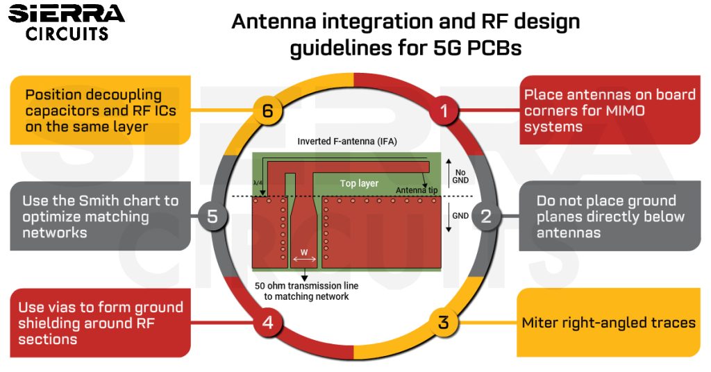
1. Place MIMO antennas on board corners
Antennas operate in different modes and require specific placements to radiate effectively. As an RF engineer, you need to ensure that the antenna radiation is not picked up by neighboring devices. Consider these RF PCB design guidelines for 5G for efficient antenna integration.
10 design tips for successful antenna integration in RF PCBs
- Place the antenna at one corner of the PCB to provide clearance in five spatial directions, with the feed in the sixth direction. This placement minimizes interference from other components and maximizes the antenna’s exposure to free space.

- Select the appropriate antenna that best fits your layout. For optimal performance, follow the manufacturer datasheet’s reference design.
- If there are multiple antennas, employ them in separate corners of your board.

- Adhere to antenna keep-out area for each layer to ensure it remains free of metallic objects. Do not place components or mounting screws within this designated space to prevent interference.

- Avoid placing a battery, LCD, or metal components such as HDMI and noisy high-speed switching components close to the antenna. These components can introduce unwanted noise, block the radiation path, or alter the electrical characteristics of the ground plane.
- Position the components below an 8-degree line drawn from the base of the embedded antenna to maintain the ideal distance between them.


- Isolate the nearby antennas by at least 10 dB for up to 1 GHz and 20 dB for up to 20 GHz. To achieve this, rotate the antennas 90 or 180 degrees apart.
- Align the antenna with the final product orientation to maximize radiation in the desired direction.
- Do not cover the antenna with a metallic enclosure, as antenna signals can’t travel through it. If the product has a metallic casing or shield, ensure it does not cover the antenna.
- Avoid placing the antenna close to the plastic in the industrial design. Plastic has a higher dielectric constant than air, and its proximity to the antenna results in a higher effective dielectric constant. This, in turn, increases the electrical length of the antenna trace and reduces the resonant frequency.
Learn every step to create a high-frequency communication board layout. Download our RF and Microwave design guide now!

RF & Microwave Design Guide
8 Chapters - 44 Pages - 60 Minute ReadWhat's Inside:
- Basics of RF and microwave board design
- Choosing RF materials
- Trace, grounding, via, and stack-up design
- Component selection and placement
- Testing and isolation requirements to avoid interference
Download Now
2. Provide a wide ground plane beneath radio frequency traces
The ground plane serves as the return path for the RF signals. To ensure optimal RF performance, the return path should be uninterrupted and as broad as possible.
Return currents seek alternative paths when the ground plane is disrupted, often creating current loops and introducing unwanted inductance, causing significant attenuation. Additionally, a narrow ground plane fails to function like a microstrip, potentially leading to increased signal leakage.
11 strategies to design solid ground planes in RF PCBs
- Factor in the size and space of the ground plane, considering adequate space for communication wires, batteries, and power sources. The antenna’s ground plane impacts the radiation and is related to the operating frequency.
- Do not route non-RF traces over RF traces in the ground plane. Dedicate an entire layer specifically for the ground.
- Follow the antenna manufacturer’s recommended ground pattern.
- Fill unused areas on the top and bottom layers with the ground and connect them to the ground plane using vias with a minimum spacing of λ/20 of the operating frequency.
- Maintain sufficient ground clearance from the antenna.
- Utilize isolation structures such as ground pours, via fences, and waveguide routing techniques to shield RF-sensitive components on the board. Here’s a quick summary of different isolation structures.
| Isolation structure | Advantages | Disadvantages |
|---|---|---|
| Shielding can | Excellent isolation if the gaps are minimal | -Bulky -Custom design required |
| Ground pour | Creates a CPW for RF antenna feedlines with high isolation | -Takes up board space -Not ideal for compact and densely populated PCB designs |
| Via fences | Offers similar isolation as ground pour with more space-efficiency | -Lower isolation -Narrowband only -Low cut-off frequency |
| Bandgap structures | Provides moderate to high bandgap isolation for particular bandwidth. Ideal for high frequencies and occupies less board space | -Performance is highly dependent on unit cells geometry. - Weaker to no blocking at other frequencies. |
| Waveguide routing | Provides high isolation, and mode selection for bandwidth specific routing | -Requires more board space -Only appropriate for most critical lines |
- Avoid using two-layer boards for the chip scale package (CSP), as routing signals through the second layer complicates creating an uninterrupted ground plane for RF signals.
- Do not split grounds, as they can create current loops. Current loops can act like antennas, picking up and emitting EMI, which can cause circuit interference.
- Provide a wide ground plane beneath the RF trace. This helps prevent parasitic transmission modes and reduces leakage permitted by narrow ground planes.
- Shield all traces with the bottom ground plane, along with the top ground plane and vias connecting the two to ensure EMC.
- Cover the corners of the power plane with vias connecting to ground planes on either side. This helps prevent any unintended EMI from the power plane through board edges.
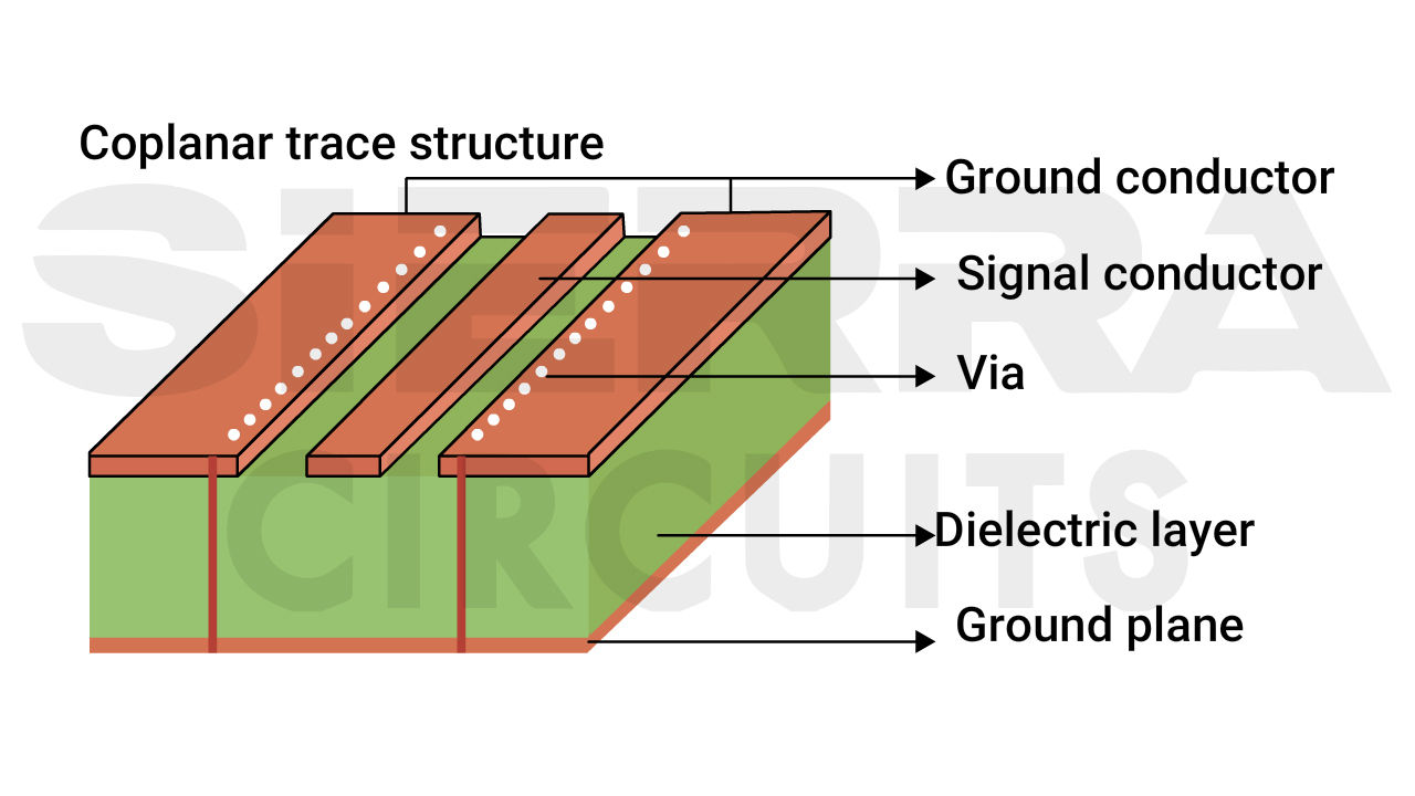
3. Miter right-angled traces to ensure constant impedance
The two most popular transmission line types used for 5G applications are microstrip lines and coplanar waveguides (CPWG), mainly because they are simple to design and cost-effective.
The effective dielectric constant of a microstrip on the same substrate is higher than that of a coplanar waveguide, resulting in a more compact layout.

Whereas, CPWG is preferred over microstrip because it offers better RF trace isolation, improved EMI performance, easier grounding for shunt elements, reduced cross-talk, and lower loss at very high frequencies.
To learn more about the benefits of using CPW for high-frequency applications, see microwave PCB material selection and CPW for signal integrity.
12 tips for optimizing RF trace design in 5G devices
- Make sure the characteristic impedance of your RF trace is 50 Ω. This helps prevent signal reflections that degrade the signal-to-noise ratio (SNR) and potentially desense the radio receiver. This ensures a good voltage standing-wave ratio (VSWR) for optimal performance.

- Select the appropriate transmission line structure (microstrip or CPWG).
- Maintain a consistent width along the trace for a constant characteristic impedance. For CPWG, keep a steady gap between the RF trace and the adjacent ground.

- Ensure that the gap between the CPWG grounds is less than the height of the substrate. If not, the trace may exhibit typical microstrip transmission line properties.
- Provide a ground pour area on either side of the trace that is wider than the gap between the grounds for the CPWG.
- Keep the transmission line straight to avoid losses due to bends.

- Ensure the battery cable or mic cable does not cross the antenna trace.
- Minimize the length of the RF trace to prevent signal attenuation caused by the traces and substrate underneath.
- Do not place any traces close or parallel to the RF trace to prevent signal coupling.
- Miter right-angled traces to ensure constant impedance across the bends.

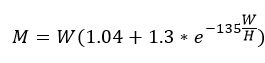
where,
M- mitering width
W- RF trace width
H- substrate height
- Verify that the RF trace maintains a 50-ohm characteristic impedance using the impedance calculators to determine the required trace width and gap within a given stack-up.
- Avoid stubs or branching in the RF trace, as they introduce reactive impedance and disrupt impedance matching.
Sierra Circuits designed an RF PCB with three sensors primarily used in IoT applications. The 4-layer board operating at 2. 4 GHz frequency included an air quality sensor, a light sensor, and a humidity sensor.
To avoid undesired results, it was critical to isolate these sensors from the rest of the circuitry. To achieve this, our RF engineers used L-shaped cut-out regions.

Further, they placed the sensors in the opposite direction and away from the antenna to mitigate the risk of interference.
Identifying the specific RF board requirements and considerations to eliminate power and noise in sensor circuitry helped us to manufacture a board with the desired performance.
Sierra Circuits fabricates high-quality RF and microwave boards with operating frequencies ranging from 10 MHz to 30 GHz. See RF and microwave PCB manufacturing services to learn more.
4. Use vias to form ground shielding around the radio section
Vias are essential for signal connectivity across layers in multilayer boards but can introduce significant parasitics that disrupt RF performance if misused. For instance, sharing a via between different circuit sections increases common-mode noise.
Placing a ground via far from a shunt component alters the component’s impedance at the trace, causing impedance mismatch. At high frequencies, parasitic inductance in vias causes signal loss in the RF path. We have listed a few RF PCB design guidelines for 5G to ensure reliable vias.
8 via design strategies to ensure signal integrity
- Use vias to form ground shielding around the RF section whenever possible.
- Incorporate numerous ground vias with a maximum spacing of λ/20 between ground fills on the top and inner ground layers.
- Place vias evenly along both sides of the transmission line to isolate noise from nearby traces or ground layers.
- Position ground vias right next to pins/pads on the top layer and add more vias whenever possible. When multiple ground vias are placed in parallel, the total parasitic inductance of the via network is reduced compared to having just a single via.
- Provide dedicated vias for each pin or pad of RF ICs. Never share a via between multiple pins or pads.
- Do not route the RF trace to a different layer using vias.
- Include a sufficient number of vias for the central ground pad in the QFN package to minimize parasitic inductance and ensure the IC shares the same ground as the rest of the board.
- Utilize ADS, Pathwave, Ansys, and HFSS, which are flagship tools that model and simulate wave propagation of the microwave and RF designs.
To learn how to overcome common radio PCB via design challenges, read 4 RF PCB via design challenges with layout solutions.
5. Prefer higher layer count stack-ups to facilitate mixed-signal designs
In radio frequency, PCB stack-up design, layer count plays a critical role. Boards with low layer counts are typically not suitable for RF applications due to limited space for power, ground, and signal layers while meeting target impedance needs. Hence, opting for a higher layer count board is essential.
8 RF PCB design guidelines for 5G stack-up
- Prefer higher layer count stack-ups to facilitate mixed-signal designs.
- A 6-layer board (as shown below) can accommodate digital signals on two signal layers and RF signals on the top layer. Placing adjacent power and ground planes on the same side of the core improves decoupling due to increased capacitance.
6-layer arrangement of radio frequency circuit boards:
| 6-layer board RF PCB stack-up | |
|---|---|
| Top layer | RF IC, RF components, RF traces, antennas |
| Layer 2 | Ground plane 1 |
| Layer 3 | Power plane |
| Layer 4 | Digital signal plane |
| Layer 5 | Ground plane 2 |
| Bottom layer | Controlled impedance differential pairs for digital interfaces |
-
- Prefer using a four-layer PCB over two-layer boards. They are slightly better for RF designs than 2-layer boards as they offer a full ground and power plane, making signal routing simpler.
4-layer RF build-up:
| 4-layer board RF PCB stack-up | |
|---|---|
| Top layer | RF IC, RF components, RF traces, antennas, decoupling capacitors, and other signals |
| Layer 2 | Ground plane |
| Layer 3 | Power plane |
| Bottom layer | Non-RF components and signals |
-
- Choose two-layer boards only for simpler and cost-effective applications.
2-layer radio frequency stack-up:
| 2-layer board RF PCB stack-up | |
|---|---|
| Top layer | RF IC, components, RF traces, antenna, decoupling capacitors, power, and other signals |
| Bottom layer | Solid ground plane |
- When choosing a two-layer board, opt for a thinner stack-up. The RF trace width for a given characteristic impedance is directly proportional to the substrate height. Thicker PCBs (greater than 0.8 mm) require wider RF traces, complicate signal routing, and trigger parasitic wave modes.
- Place thick traces on the top layer for routing the power supply in two-layer boards.
- Ensure a solid ground plane below the radio-frequency section if a full ground plane at the bottom layer isn’t feasible.
- Place high-frequency signals adjacent to ground planes. Power planes should be next to ground planes for enhanced decoupling and low-frequency signals on non-critical layers for signal integrity.
- Choose materials with low dielectric constant and low loss tangent, such as FEP, PTFE, ceramic-filled PTFE, and high-speed non-PTFE. They offer outstanding electrical properties and heat resistance (over 200°C) for high-power or longer-range applications.
- If cost is not an issue, consider PTFE with fiberglass as the top material choice for RF PCB applications. However, if cost reduction is a priority, choose PTFE with ceramic coating, which requires a simpler fabrication process.
- Use laminates for outer layers and more economical epoxy glass laminates for inner layers for cost effectiveness. Rogers materials like RT/duroid 5880, despite their higher cost, reduce power losses by 50%, ensuring high performance beyond 20 GHz with a consistently low dielectric constant.
- Use regular FR4 for low-power and low-range ISM band applications like IoT, wifi, and Bluetooth.
- Obtain a sample stack-up design from your fab house before designing the RF layout for 5G and IoT devices.
To learn about RF PCB design parameters, see 9 factors that impact RF PCB design and tips to resolve them.
6. Use the Smith chart to optimize the matching network
It becomes essential to provide an antenna-matching network as its impedance can vary due to multiple factors like plastic enclosure, substrate differences, ground variation, and other components in the antenna’s proximity.
Moreover, unintentional small stubs across the RF trace can act as capacitors or inductors, changing the impedance and requiring the antenna to be returned.

12 tips for designing matching networks in 5G boards
- Use RF matching components and appropriately sized transmission lines to tune the antenna to 50 Ω. Keep the transmission line as short as possible to minimize losses.
- Match the trace length from the antenna as per the datasheet when incorporating a matching network into your design.
- Use the Smith chart to design and optimize the matching network.
- Include a provision for an antenna matching network, as several factors in the antenna’s proximity can alter its impedance and require retuning.
- Have a provision for a PI or T network with three components if the antenna impedance is unknown. You can do this by populating 0 ohms in the series components and leaving the shunt components unloaded. This allows for easy adjustment to any necessary matching network topology later.

- Verify the antenna matching network performance with the final plastic enclosure in place.

- Measure the impedance at the exact location where the components will be installed.
- Position the shunt components directly onto the RF trace. This avoids the use of lengthy traces.
- Select capacitors with a series resonant frequency that is at least double the frequency of operation.
- Choose inductors with a self-resonant frequency that is at least twice the frequency of operation.
- Employ a matching network with at least four components for high-data-rate applications such as voice recognition over remote control. Two of these components will be utilized for radio tuning, while the remaining two will be allocated for antenna tuning.
- Include an additional component footprint in the design to facilitate future mitigation of EMI radiation in a new product. These extra components can be utilized to implement filters for out-of-band operation.
- Use a vector network analyzer (VNA) to probe the test circuit on the board and determine the impedance at the antenna input. Measuring the S-parameters and VSWR bandwidth helps analyze the antenna’s performance.
To learn how to address impedance mismatches in a microwave board, see microwave PCB design challenges and ways to overcome them.
7. Position the decoupling capacitor and RF IC on the same layer
Decoupling capacitors are used to filter the noise from the IC. The power supply noise can elevate the frequency synthesizer’s phase noise, degrading signal quality. This can cause undesired interference and radiations exceeding regulatory limits. Further, it causes an increase in packet errors and reduced sensitivity in the receiver end.
The following RF PCB design guidelines for 5G help mitigate signal degradation at high frequencies and minimize the overall error rate during data packet transmission over the network.
5 best practices to reduce power supply noise
- Place components as close to the supply pin as possible, with the smallest-value capacitor positioned nearest to the power supply pin.

- Position the decoupling capacitor on the same layer as the IC. If placing all capacitors on the same layer isn’t feasible, prioritize smaller values.
- Ensure the power supply flows directly through the decoupling capacitors to the IC’s power supply pin. Avoid vias in this path.
- Ground each decoupling capacitor using dedicated vias.
- Employ separate vias to establish the connection between the power pins and the power plane.

For more on decap, read decoupling capacitor placement guidelines for PCB design.
8. Opt for high-Q capacitors and inductors
Choosing the right capacitor and inductor is a critical step in your RF design for use in the matching network, crystals, DC blocks, and power supply decoupling.
7 tips to choose capacitors for your RF printed boards
- Utilize only C0G/NP0 ceramic capacitors for matching networks to ensure consistent performance across different temperatures. They also maintain consistent clock timing and RF frequency across temperatures.
- Choose capacitors that operate reasonably below the self-resonant frequency (SRF) of the matching network.
- Employ X5R or X7R multilayer ceramic capacitors for decoupling, which offers cost savings. The accuracy of C0G capacitors may not be necessary for this application. Opt for low equivalent series resistance (ESR) capacitors for efficient decoupling.
- Select decoupling capacitor values that have an SRF at the noise frequencies.
- Use capacitors with high-quality factor (Q factor).
- Utilize smaller component package sizes (0402 or 0201) as they exhibit lower parasitic reactance.
- Opt for a capacitor with an SRF close to the operating frequency and a low ESR when adding a DC block to an already-matched RF trace. This ensures the capacitor’s effective reactance becomes zero at SRF, thereby maintaining impedance matching without alteration.
5 techniques to select inductors for your radio frequency design
- Opt for high-Q inductors with an SRF well above the operating frequency for matching networks.
- Check the datasheet of RF ceramic inductors to assess if the Q is sufficient at 2.4 GHz before using it. These inductors offer cost-effectiveness and high SRF but may exhibit lower Q and current capacity, especially in higher-value variants.
- Choose inductors with an SRF close to the noise frequency for power supply filtering. This ensures a low-impedance path to the noise signals, diverting them away from the power supply lines and preventing them from reaching the sensitive components.
- Prioritize wire-wound inductors over ceramic inductors for high inductance values. Wire-wound inductors offer high Q and current capacity due to their low DC resistance.
- Avoid placing inductors parallel and in close proximity to each other, as it causes crosstalk due to mutual inductance. Instead, position inductors orthogonal to each other.
To learn the ways to avoid crosstalk in your layout, see handling crosstalk in high-speed PCB designs.
9. Avoid placing test points on RF traces
To validate the accuracy of component assembly, transmit-power level, packet error rate (PER), receiver sensitivity, and a few RF parameters are assessed. Traditional testing methods like in-circuit testing are unsuitable for evaluating the RF section since it is discouraged to position a test point directly on the RF trace.
5 DFT rules RF designers should know
- Avoid placing test points on the RF trace, as they act as stubs and affect impedance matching.

- Use BLE testers to test the full radio path indirectly. The golden board (GB) is a cost-effective alternative for testing, measuring packet error rate (PER) at pre-calibrated attenuation levels.
- Measure antenna radiation patterns using anechoic chambers. Conduct PER assessments in both directions, from the device under test (DUT) to the GB and vice versa.
- Maintain a controlled environment, such as a Faraday cage or shielded room, for all radiated tests. Configure the test equipment to account for loss over the air and through cables. Ensure consistent distance and orientation between the transmitter and receiver for all devices.
- When routing branches for the RF connector, arrange the trace leading to the antenna and the trace going to the branch so that isolating one trace does not result in the other trace acting as a stub.

For more design for testing rules, download our handbook.

Design for Testing Handbook
7 Chapters - 28 Pages - 45 Minute ReadWhat's Inside:
- PCB testing strategies
- Guidelines to design and place a test point for FPT
- Directives to make your board ICT compatible
- Benefits and drawbacks of various testing methods
- Defects that you can identify through board testing
Download Now
Key takeaways:
- Consider regulatory standards, operating frequency band, radiation pattern, and gain during antenna integration in RF PCBs.
- Select between various antenna types such as monopole, dipole, inverted F-antennas and MIFA based on the application.
- Use vias to form ground shielding around the RF section, but avoid introducing parasitics that disrupt RF performance.
- Opt for higher RF PCB performance, allowing for controlled impedance routing and better shielding.
- Design matching networks with PI or T network provisions for flexibility.
- Ensure power supply flows directly through decoupling capacitors to the IC, avoiding vias in this path.
- Utilize C0G/NP0 ceramic capacitors for the matching network and crystal load.
- Do not place test points on the RF trace, as they act as stubs and affect impedance matching.
Consider these RF PCB design guidelines for 5G to build a reliable circuit board.
The success of an RF antenna design for 5G and IoT devices requires engineering expertise and a deep understanding of the complex dynamics between hardware, software, and electromagnetic principles.
From antenna selection and placement intricacies to impedance matching, signal integrity, and adherence to regulatory standards, every aspect of PCB design for 5G and IoT demands meticulous attention to detail to ensure a robust RF board.
Need help designing an RF circuit board? Post your questions on our PCB forum, SierraConnect. Our design experts will resolve them.


Download the RF & Microwave Design Guide_Sierra Circuits.pdf (1.6 MB)
How can the same antenna be designed to function effectively for both transmitting and receiving signals?
What strategies do you use to create a low-impedance ground plane in RF boards?
An antenna is designed to be resonant at specific frequencies, which means it can efficiently transmit and receive electromagnetic waves at those frequencies. The key to using the same antenna for both purposes lies in a device called a T/R (transmit/receive) switch.
When the system is in transmit mode, the T/R switch ensures that the transmitter is connected to the antenna, allowing it to send out signals. When in receive mode, the switch connects the antenna to the receiver, enabling it to pick up incoming signals. This switching mechanism prevents the transmitter and receiver from being active simultaneously, which could otherwise lead to damage.
Lower-power systems typically use PIN diodes in their T/R switches due to their fast switching speeds and reliability. Higher-power systems, on the other hand, use relays because they can handle greater power levels without damage.
By incorporating a T/R switch, the system ensures that the same antenna can be effectively and safely used for both transmitting and receiving.
Extensive use of copper in planes and pours is a fundamental approach, although it’s important to note that due to the skin effect, simply adding more copper isn’t always sufficient.
Utilizing highly conductive materials such as gold and silver for surface finishes can significantly enhance performance, with common finishes including electroless nickel immersion gold (ENIG), which offers excellent conductivity and corrosion resistance.
Implementing coplanar waveguide and microstrip lines is preferred, with CPW used inside the board and microstrip lines on the surface, ensuring optimal signal integrity. Additionally, ensuring precise dimensions and accuracy in the design and manufacturing process is crucial to maintaining a low-impedance ground plane.