Contents

On-demand webinar
How Good is My Shield? An Introduction to Transfer Impedance and Shielding Effectiveness
by Karen Burnham
Christopher Young, President of Young Engineering Services, discussed the common aerospace circuit board design challenges and ways to overcome them at PCB West 2023.
Highlights:
- Choose materials such as FR408 and 370HR for aerospace designs.
- Aerospace PCBs often have layer counts ranging from 12 to 22 layers.
- IPC-2220 series and IPC-6612 provide guidelines for aerospace applications.
- Closely couple ground planes with power planes within approximately 4 mil spacing to solve electromagnetic issues.
Watch the full video to learn more.
What challenges do you face while designing aerospace and defense PCBs?
Christopher Young: Time and money are the biggest enemies when it comes to aerospace circuit board design. The extensive certification and testing processes can be extremely daunting and time-consuming. This can squeeze your window for design and development.
Therefore, it’s essential to get things right on the first try to reduce the need for rework. Conducting thorough front-end simulations, forethought how the system will behave, and learning its unique characteristics are extremely critical for aerospace and defense applications.
For aerospace PCB design tips, see 14 aviation and aerospace design rules for high reliability.
Can you tell us some important layout design techniques that you follow?
Christopher Young: When it comes to layout design techniques, explore the PCB West and PCB East conferences. These events host experienced professionals, including Rick Hartley, Lee Richey, and many other renowned experts who are authorities in the field of design principles.
Avionics circuit boards entail stringent requirements for aspects like annular rings, accuracy, and drill holes. Further, meeting elevated dielectric strength standards is crucial in such cases.
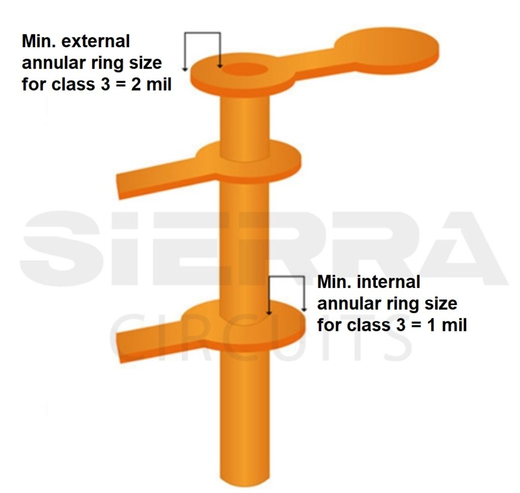
Connect with experts in their respective fields and engage in discussions. For instance, when discussing power distribution systems with Lee Richey, he’ll emphasize the importance of closely coupling the power plane with the ground plane to achieve low impedance across a broader frequency bandwidth. On the other hand, when you converse with Rick Hartley, he’ll focus on the systems engineering approach and the fundamental principles that must be followed to ensure compliance with established rules and standards such as IPC 6012-ES.
IPC Class 3 Design Guide
8 Chapters - 23 Pages - 35 Minute ReadWhat's Inside:
- IPC guidelines for manufacturing defects
- IPC standards for assembly processes
- Common differences between the classes
- IPC documents to set the level of acceptance criteria
Download Now
What are the PCB materials that you choose for your aerospace designs?
Christopher Young: Avionics is no exception to the trend of miniaturizing components and increasing power density. As a result, you have a couple of material options to consider. There’s the high-performance FR408 material, known for its impressive glass transition temperature and suitable properties. It can be an ideal choice for high-power and high-density designs.
On the other hand, if your design doesn’t require such high power or if you’re pushing the limits of your board’s aspect ratio, many companies opt for the more cost-effective 370HR material. This choice is often driven by the 370HR material’s slightly improved z-axis coefficient of thermal expansion.
In the automotive sector, we’re observing a promising development. The EM370 material is gaining traction due to its elevated glass transition temperature, comparable to FR408, and its reduced z-axis expansion. The 370HR material is proving valuable for smaller designs by providing more flexibility for aspect ratios, which contributes to improved production yields.
Is there anything specific to via design you would like to share?
Christopher Young: It’s crucial to recognize that ground via behaves like an inductor, whereas a series via acts as a capacitor. These distinctions are significant as vias serve more than just providing vertical connections between PCB layers, especially as technology advances in the aircraft industry.
For instance, with the current deployment of AFDX Ethernet at 1000BASE-T speeds and the TTGB technology on aircraft like the Boeing 777 or the Artemis program within the Orion capsule, they are utilizing 10-gigabit Ethernet. This goes beyond the typical 100BASE Ethernet speeds and even involves amplitude modulation within the pulse frames.
Thus, the placement and design of vias, as well as the overall PCB structures, become critical factors that can significantly impact the performance of these advanced systems.
What are the key factors to consider when selecting components for aerospace and defense PCBs?
Christopher Young: One of the primary considerations in choosing circuit board components is the temperature range they can handle. Military-grade components can be quite challenging to find because they’re designed to operate in extreme conditions, ranging from -55°C degrees to 175°C.
When you choose standard avionics products for use in commercial aircraft, it’s crucial to address the typical temperature requirements for the electronics bay. This environment requires the ability to withstand freezing temperatures as low as -55°C while also enduring excessive heat of +70°C.
A significant challenge in aerospace PCB design lies in the fact that many industrial components are rated for operation only as low as -40°C. Therefore, you need to understand how to derate components for use beyond their specified temperature range and establish screening and testing procedures to ensure their suitability for your application.
Also, packaging is a critical consideration. At high altitudes, the temperature in the electronics bay can drop to as low as -55°C. However, as you descend and approach your landing, the temperature can drastically change, especially if you’re landing in a place like Phoenix. During the descent, you may experience a temperature increase of up to 100°C. The same temperature fluctuations occur during takeoff. This results in significant temperature ramps, sometimes 5 to 8°C per minute. This ramp is a substantial and rapid change to manage in avionics systems.
You have to consider that aircraft are continually taking off and landing throughout the day. Therefore, the structural integrity of the components is crucial to support the compression and expansion of the PCB as it experiences rapid temperature changes in these demanding operational environments.
What are the IPC standards that you follow to ensure your design matches the industry standards?
Christopher Young: When it comes to design standards, we often refer to IPC, particularly the IPC-2220 series and IPC-6612. There have been new updates to IPC-6612, such as the ES for space applications and the EM for materials.
These standards serve as guidelines to ensure that your designs are aligned with industry best practices. It can further help you stay on the right track and avoid venturing into uncharted territory. It can also prevent you from making design choices that deviate from established norms.
Furthermore, it’s highly beneficial to enrich your knowledge by conversing with and learning from experts like Lee Richey, Daniel Beeker from NXP, Rick Hartley, and others in the field, such as Steven Chavez at Siemens.
These individuals have dedicated a significant portion of their careers to immersing themselves in the intricacies of these specifications. It’s wise to familiarize yourself with their work and recognize them as the guardians and champions of these standards. While they may not be directly affiliated with IPC, they play a pivotal role in ensuring that the insights and best practices related to these specifications are effectively communicated and understood throughout the industry.
What are the new changes in IPC class 3 standards PCB designers should know?
Christopher Young: It’s becoming increasingly evident that we need to make changes in the testing process, especially concerning coupon testing. The coupons used in these tests should play a more integral role. It’s a known issue that certain standards have identified deficiencies in this regard. Typically, coupons have been somewhat sidelined and not considered a core component in PCB design.

Traditionally, companies have conducted coupon testing, but these tests haven’t always provided an accurate representation of the actual PCBs. It’s similar to working with silicone, where the best results are obtained in the center of the silicone disc rather than the outer edges. This discrepancy highlights the need for improved testing practices.
As things progress, there’s a noticeable shift in the way testing is approached. People are increasingly migrating some of their test coupon structures directly onto the circuit boards. This shift aims to provide a more accurate representation of how the board is actually constructed.
The days of accepting a ±20% tolerance range as sufficient are behind us. Now, the focus is on achieving a tighter tolerance of ±3% of nominal values.
This increased precision applies to various aspects of PCB design, including impedance, drill holes, and annular ring dimensions. There’s a growing emphasis on verification and validation from a system standpoint. While others may delve into intricate details, the primary concern lies in ensuring the accuracy and reliability of the design.
Is there a stack-up design strategy that you follow to make your applications reliable and EM-compliant?
Christopher Young: The PCB stack-up strategy revolves around closely coupling the ground planes with the power planes. It’s crucial to gain a thorough understanding of the ripple voltage that can affect the power rails. This understanding can help determine the level of coupling required.
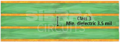
As Lee Richey often highlights, the goal is to effectively sandwich a ground plane between power planes, typically within about 4 mil. This relationship is widely recognized and well-documented across the industry. A well-coupled power plane solves numerous electromagnetic issues.
Could you discuss some strategies to maintain signal integrity and power integrity in aerospace and defense circuit boards?
Christopher Young: A major concern revolves around the usage of quick fixes to address signal integrity issues. There has been a significant discussion about incorporating ferrite beads.
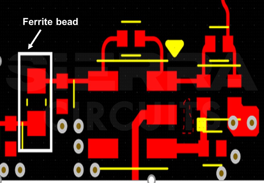
A ferrite bead is essentially an inductor, originally intended for use as a filter element rather than as a solution for EM challenges. In the past, some stumbled upon this solution and found that it appeared to work. Consequently, there’s been a push for its widespread adoption.
However, the reality is that relying on ferrite beads as a universal solution isn’t the right approach. The key is to design your power distribution system to align with your electrical requirements. This is the foundation for maintaining both power integrity and signal integrity.
Having a well-designed power distribution system can proactively prevent numerous problems and challenges in aerospace PCB design. In this case, an ounce of prevention is indeed worth a pound of cure.
What are the design challenges of using HDI technology in aerospace PCBs?
Christopher Young: HDI PCBs haven’t been widely implemented at the board level in avionics. The challenge lies in how to seamlessly integrate high-density technology with our current fabrication processes. However, you can look forward to the potential for additive processes.
One such process is the 3D printing of circuit boards to revolutionize this technology. It can be a game-changer and make HDI technology more accessible and applicable in avionics.

HDI PCB Design Guide
5 Chapters - 52 Pages - 60 Minute ReadWhat's Inside:
- Planning your stack-up and microvia structure
- Choosing the right materials
- Signal integrity and controlled impedance in HDI
- Manufacturing considerations for higher yields
Download Now
What is the number of layers, copper thickness, and surface finishes used for aerospace PCBs?
Christopher Young: In aerospace, it’s quite common to come across PCBs with 12 to 22 layers. This helps in the effective coupling of power and ground planes. By including these additional layers, they create a robust power distribution system, reducing the likelihood of EMC issues.
When closely coupled to the ground plane, the power plane exhibits similar characteristics to ground planes. This is from a signal perspective and in terms of AC impedance. This similarity enables the use of an asymmetric stripline structure between a power plane and a non-coupled ground plane without causing any problems.
The choice of circuit board surface finishes depends on the application. In avionics, particularly with airborne radar-type equipment such as TCAS, transponders, DME, and NAV-COM radios, the surface finish becomes a crucial consideration. Using emergent silver finishes on high-power RF components can lead to rapid material migration, which is undesirable.
In a recent design project, we chose immersion tin to address material migration issues. Some might wonder why we didn’t opt for gold plating instead. The reason is that gold plating relies on a nickel layer underneath to provide support and reinforcement. However, this nickel layer introduces excessive loss, especially when dealing with high-power RF. As a result, it leads to significant impedance mismatches caused solely by the choice of surface finish.
Interestingly, these issues may not become apparent at lower power levels. You could use a VNA and not detect any significant problems. However, when you begin transmitting high-power RF pulses (1000W), you’ll notice substantial distortions. This can be quite perplexing until you realize that it all comes down to the choice of surface finish used in the design.
Key takeaways:
- Conduct thorough front-end simulations to understand the system behavior of aerospace projects.
- For avionics applications, meeting Class 3 standards and dielectric strength requirements is essential.
- EM370, with its slightly improved z-axis coefficient of thermal expansion, is more cost-effective for use in aerospace applications.
- Designing a power distribution system to meet electrical requirements to maintain power and signal integrity is crucial.
- Immersion tin can be a preferable surface finish over gold plating due to its impact on impedance.
Incorporate these valuable recommendations from Christopher Young to overcome aerospace PCB design challenges.
About Pooja Mitra : Pooja Mitra is an electronics and communication engineer. With an experience of over three years in the PCB industry, she creates industry-focused articles that help electrical and PCB layout engineers.




Start the discussion at sierraconnect.protoexpress.com