Tools for Designers:
PCB Stackup Designer
Start Building Your Stack-UpPCB stack-ups represent the construction of multilayer circuit boards. They provide vital information like material thickness and copper weight required to fabricate a board. Stack-ups also determine the trace width, trace spacing, and reference planes of controlled impedance traces. These layer stacks are sometimes called build-ups. Circuit boards with accurately stacked layers offer improved signal integrity by reducing electromagnetic emissions and crosstalk.
Sierra Circuits’ Stackup Designer provides precise options for cost-optimized build-up structures. It also includes an impedance calculator to get the desired impedance and trace and space values on any signal layer.
Features of our Stackup Designer
Our tool has the following features that will help you to design a reliable build-up:
- It has a library of stack-up templates. The templates include single and sequential lamination build-ups (HDI-1, HDI-2, HDI-3, and HDI-4). The digits here represent the number of sequential laminations. For example, HDI-2 has core plus 2 laminations.
- It includes a variety of material databases suitable for a wide range of applications (low to very high-speed).
- It is based on the material selection, it automatically chooses the type of board construction (foil or core type).
- To meet the requirements of high-speed designs, the tool is linked to our 2D field solver-based impedance calculator which allows you to design any controlled impedance traces.
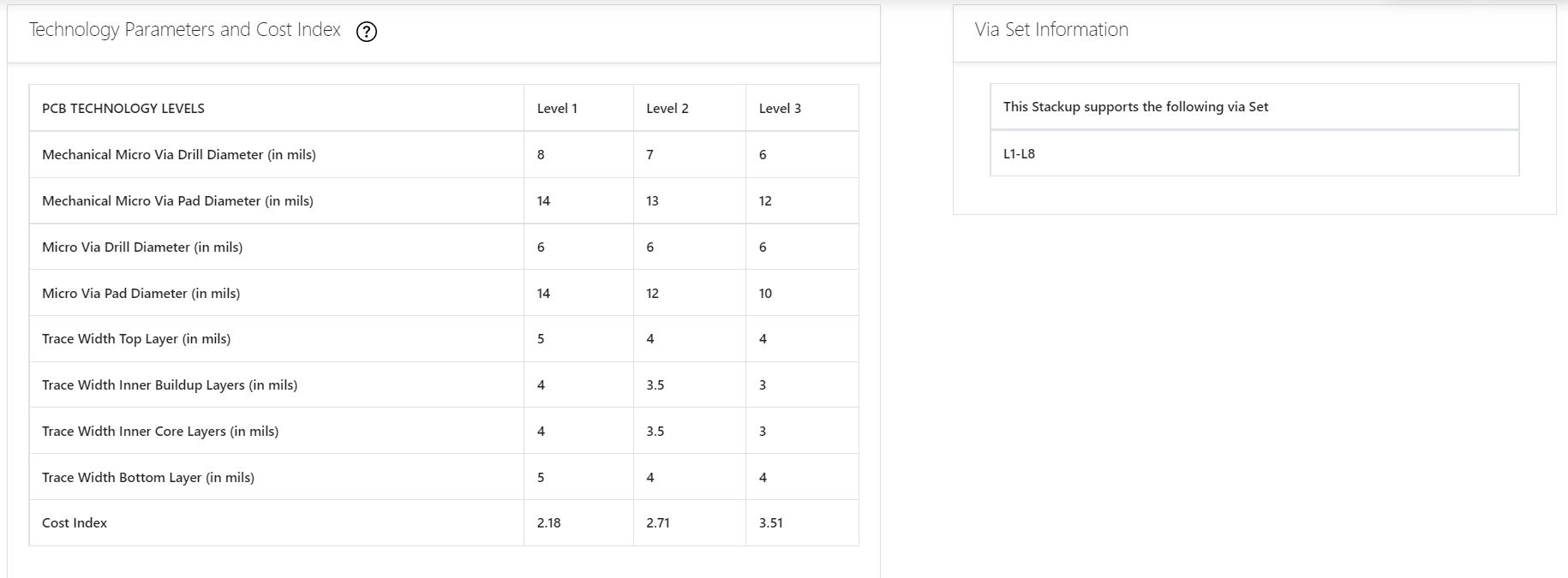
- Offers 3 technology levels (level I/II/III) with respect to different parameters such as trace geometry, drill sizes, spacing, and cost index. Features such as drill size and trace geometry of technology level II are finer than technology level I and the features of technology level III are finer than level II.
- The cost index provides a relative idea of the cost compared to another layer order. For instance, if the cost indices for build-ups A and B are 2.6 and 1.3 respectively, then A is roughly twice as expensive as B.
- Export to IPC-2581 format.
How to use the Stackup Designer
In this section, we will describe the steps to design a board stack-up using our tool.
It has 2 sections:
- Board information
- Stack-up design method
Board information
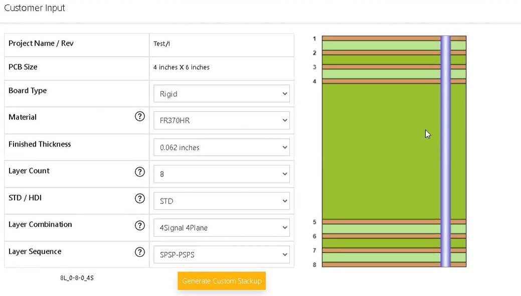
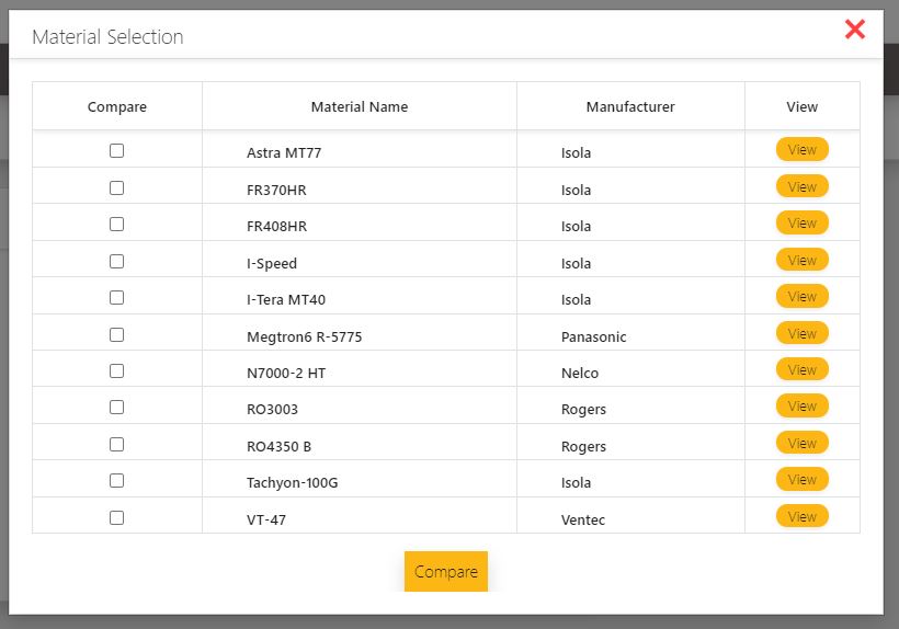
In this section, project name, revision number, PCB size (length and width), target board thickness, material, and board type are keyed in. If you are not sure about choosing the material, click on the material selector compare guide. This will allow you to view the datasheets of various materials and compare their attributes.
Stack-up design
After filling in the board info, you can move on to the stack-up design section.
Here, you will have to choose one of the following options:
- I know the number of layers in the design (Choose a Sierra standard stack-up)
- I do not know the number of layers in the design, but I have a complex BGA
Choose the first option if you know the number of layers required in your design.
Next, you will have to input the layer count along with the signal-plane layer combination and click on run stack-up generator. For demonstration purposes, we have chosen the layer count as 8 which includes 4 signal and 4 plane layers.
You will be presented with Sierra Circuits’ recommended solutions, as shown below.

Each of these options has the following information:
- Number of signal and plane layers
- Total number of layers
- Type of technology (standard or HDI)
- Number of sequential laminations required
- Board thickness
- Technology level and cost index
Click on the report to view the stack-up.
Here, you can tweak all the board attributes using the respective dropdowns except the project name and board size. If you make any changes to the board properties, hit generate custom stack-up to view the updates.
Scroll down to view the detailed stack-up.
The detailed build-up comes with the following information:
- Layer number
- Material of that layer (solder mask/copper/prepreg/core/foil)
- Layer type (signal/plane/mixed)
- Copper percentage used in the layer
- Finished thickness of the layer
- Dielectric or copper base thickness
- Copper plating thickness
- Dielectric description
- Dielectric constant (Dk) of the layer
If your design has controlled impedance traces, you can use our built-in impedance calculator. This calculator allows you to add the impedance model and compute the desired trace geometry and spacing for a target impedance.
To add the impedance models, click on ⊕ under the impedance calculator section and provide the following details:
- Signal layer
- Target impedance
- Model type (single-ended/differential pair/coplanar single-ended/coplanar differential pair)
- Reference layers
- Transmission line model
- Trace spacing
Please note that you can only choose coated microstrip models if you have solder mask layers in the build-up. The uncoated models can be selected after the removal of solder mask layers. To remove the solder mask from your design, click Ⓧ on the layer number column.
After providing the required impedance data, click on calculate impedance to view the required trace width, calculated impedance, and propagation delay.
If you would like to view other parameters such as trace thickness, inductance, capacitance, and effective dielectric constant, click on 👁 (eye symbol). This will redirect you to our impedance calculator.
Below the built-in impedance calculator, a section named, technology parameters and cost index will be displayed. This section provides the technology levels and via set information. The technology level, for a given layer stack, defines the drill size, pad size, and trace width parameters that can be used.
If you’re not sure about the number of layers required in the design, and there is a complex BGA that dictates the number of layers, choose the option I do not know the number of layers in the design, but I have a complex BGA.
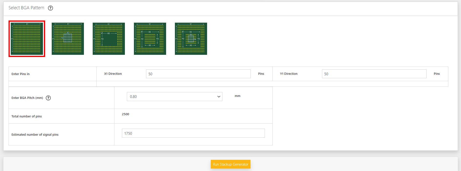
Here, you’ll have to select the applicable BGA pattern and enter the BGA pin and pitch information. Once the required data is given, the Stackup Designer automatically calculates the total number of pins and the estimated number of signal pins. You can change the estimated number of signal pins in this section.
Now, click run stack-up generator present at the bottom of the page. The tool now displays the stack-up options based on the provided input.

The recommended solutions are very similar to the previous option (Choose a Sierra standard stack-up) except for the board thickness.
Choose a suitable option and click on report. This will present a stack-up that works for your BGA.
You can also edit the build-up and the BGA attributes if required. Please remember to hit generate custom stack-up if you make any changes to the provided data.
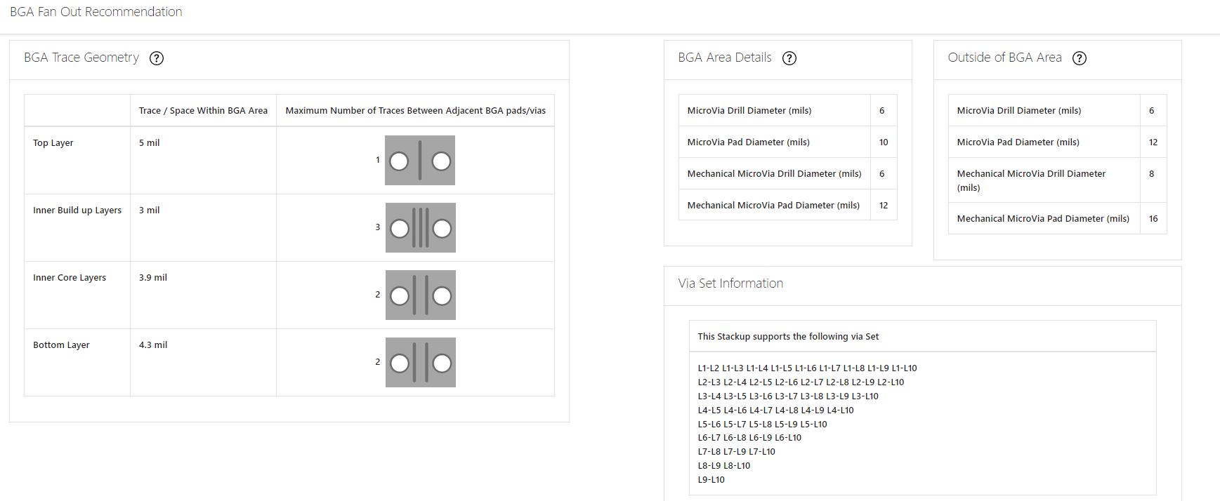
The layer details and the impedance calculation steps are the same as we saw in the previous option. The only difference is that now the BGA fan-out recommendations are available at the bottom. This provides the following information:
- BGA trace geometry and the maximum number of traces that can be routed between adjacent BGA pads and vias
- Drill and pad sizes under and outside the BGA area
- Via set information
Designing a precise and detailed stack-up at the initial stages of a layout reduces unnecessary board re-spins, optimizes the cost, and increases manufacturability. Our PCB Stackup Designer will assist you to make the right decisions before designing the layout.
Watch the demo of our Stackup Designer
Sierra Circuits has developed easy-to-use tools for PCB Designers and Electrical Engineers at every stage of circuit board development.
Fabrication, Procurement, & Assembly. PCBs fully assembled in as fast as 5 days.
- Bundled together in an entirely-online process
- Reviewed and tested by Engineers
- DFA & DFM Checks on every order
- Shipped from Silicon Valley in as fast as 5 days
Fabrication. Procurement & Assembly optional. Flexible and transparent for advanced creators.
- Rigid PCBs, built to IPC-6012 Class 2 Specs
- 2 mil (0.002″) trace / space
- DFM Checks on every order
- 24-hour turn-times available
Complex technology, with a dedicated CAM Engineer. Stack-up assistance included.
- Complex PCB requirements
- Mil-Spec & Class 3 with HDI Features
- Blind & Buried Vias
- Flex & Rigid-Flex boards

