Contents

On-demand webinar
How Good is My Shield? An Introduction to Transfer Impedance and Shielding Effectiveness
by Karen Burnham
A PCB transmission line comprises at least two conductors – one for the signal and another for its return path. Complex circuit board nets are the combinations of such simpler transmission line structures. Understanding these structures (microstrip, stripline, and coplanar) can be fruitful from the PCB design point of view, for the designer as well as the fabricator.
What are the losses in a transmission line?
Transmission line structures have different loss mechanisms. The total PCB transmission line loss is called insertion loss (αt). It is the sum of conductor loss (αc), dielectric loss (αd), radiation loss (αr), and leakage loss (αl).
αt = αc + αd + αr + αl
The effect of leakage loss can be ignored because PCBs have very high volume resistance. Radiation loss is the energy lost from the circuit due to RF radiation. This loss is dependent on frequency, dielectric constant (Dk), and thickness. For a particular transmission line, the loss will be much higher at higher frequencies. For the same circuit when using a thinner substrate with a higher Dk value, the radiation loss would be less.
In this post, we will only be discussing the transmission line losses related to the conductor loss (αc) due to signal trace resistance and the dielectric loss (αd) due to PCB dielectric which is measured in terms of loss tangent/dissipation factor.
αt = αc + αd
Characteristic impedance and loss mechanism
In our previous PCB Transmission Line series, we gave you the characteristic impedance (it is the impedance seen by the signal, independent of the frequency) of a transmission line:


R = Resistance of the line conductors per unit length (pul)
L = Inductance of the line conductors loop pul
G = Conductance (due to dielectric material) between the signal and return paths pul
C = Capacitance between the signal and return paths pul (it increases with the Dk of the dielectric)
For a uniform transmission line, R, L, G, C are the same at every point on it and therefore Zc has the same value at every point on the transmission line.
For a sinusoidal signal of frequency f (ω = 2πf) traveling in the direction over the line, expressions for voltage and current at various points and time are given by:

Where α and β are the real and imaginary components of ![]() , which is given by:
, which is given by:

At our frequencies of interest, R << ωL and G << ωC, so that:

And:
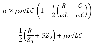
So that:

This represents a wave that travels with a propagation delay ![]() per unit length and which is attenuating as it travels along the line.
per unit length and which is attenuating as it travels along the line.
The signal attenuation factor of a transmission line of length l is:
![]()
The attenuation or signal loss factor is usually expressed in dBs.

Thus the dB loss is directly proportional to the line length. Hence, we can express the above as dB loss per unit length as:

We usually omit the minus sign, keeping in mind that it is a dB loss – always to be subtracted from the signal strength in dB.
The above is also called total insertion loss per unit length of the transmission line and written as:
![]()
Now, R/Z0 component of the loss is proportional to R, the resistance of the length per unit length and is called the conductor loss and is due to the resistance of the conductors forming the transmission line. It is represented by ‘alfa’C. GZ0 part of the loss is proportional to G – the conductance of the dielectric material and is called the dielectric loss – denoted by ‘alfa’ d.
![]()

PCB Transmission Line eBook
5 Chapters - 20 Pages - 25 Minute ReadWhat's Inside:
- What is a PCB transmission line
- Signal speed and propagation delay
- Critical length, controlled impedance and rise/fall time
- Analyzing a PCB transmission line
Download Now
Conductor loss in a PCB transmission line
![]()
Where R is the resistance of conductors per inch.
Now there are two conductors in a PCB transmission line – the signal trace and the return path.
![]()
Usually, the return path is a plane, however, the return current is not uniformly distributed over the plane – we can demonstrate that most of the current is concentrated on a strip of width three times the width of the signal trace and just underneath the signal trace.
It is possible to approximate:

So that:

Signal trace resistance in a PCB transmission line
Does the entire cross-sectional area of the signal trace participate in the signal current equally? The answer is: not always – it depends on the frequency of the signal.
At very low frequencies – until about 1MHz, we can assume that the entire conductor participates in the signal current and hence Rsig is the same as the ‘alfa’ C resistance of the signal trace, which is:

Where:
ρ = Copper resistivity in ohm-inch ![]()
W = Trace width in inches (example: a 5-mil, i.e., 0.005” trace for 50 ohms)
T = Trace thickness in inches (usually ½oz to 10oz ie. 0.0007” to 0.0014”)
For example, for a 5-mil wide trace:

For our purpose, we are interested in AC resistance at frequency f. Here, the skin effect comes into the picture. As per skin effect, the current at a frequency f travels only up to a certain depth called the skin depth of the conductor which is:

The following table gives the value of the skin depth at various frequencies:

We see from above that at 4MHz, the skin depth equals the 1oz copper thickness and at 15MHz, it equals ½oz copper thickness. Beyond 15MHz, the signal current travels only in-depth less than 0.7mils and it keeps decreasing as the frequency increases.
As we are concerned here with high-frequency behavior, we can safely assume that T is greater than the skin depth at frequencies of our interest, hence instead of using T in the formula for signal resistance, we will use the skin depth. So we now have:

We use 2δ instead of δ since the current uses all the periphery of the conductor – technically 2W can be replaced by 2(W+T).

The return signal travels in only one thickness δ along the surface nearest to the signal trace and its resistance can be approximated by:

Increase in conductor loss due to copper surface roughness at the conductor–dielectric interface
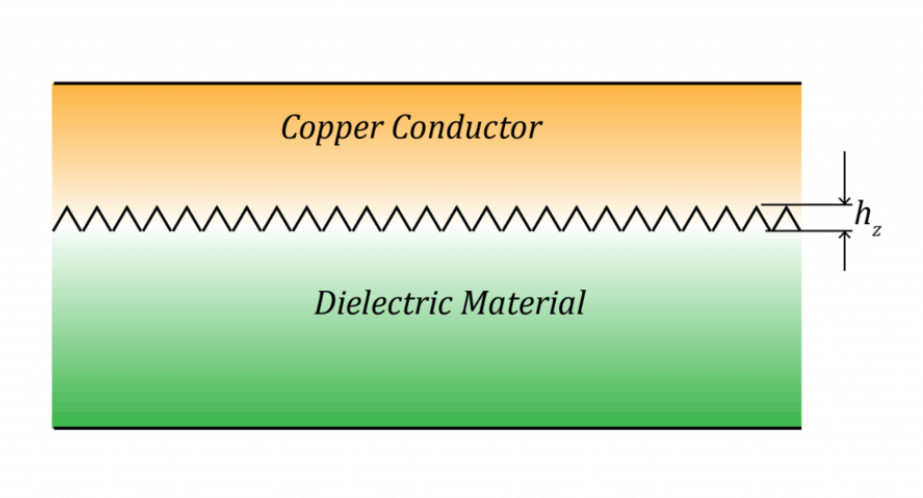
It is important to know that in a circuit board, the ‘copper conductor – dielectric interface’ is never smooth (if it were smooth, the copper conductor would easily peel off the dielectric surface); it is roughened into a teeth-like structure to increase the peel strength of conductors on the circuit board.
For a typical copper-clad laminate, the interface will look like as given below:
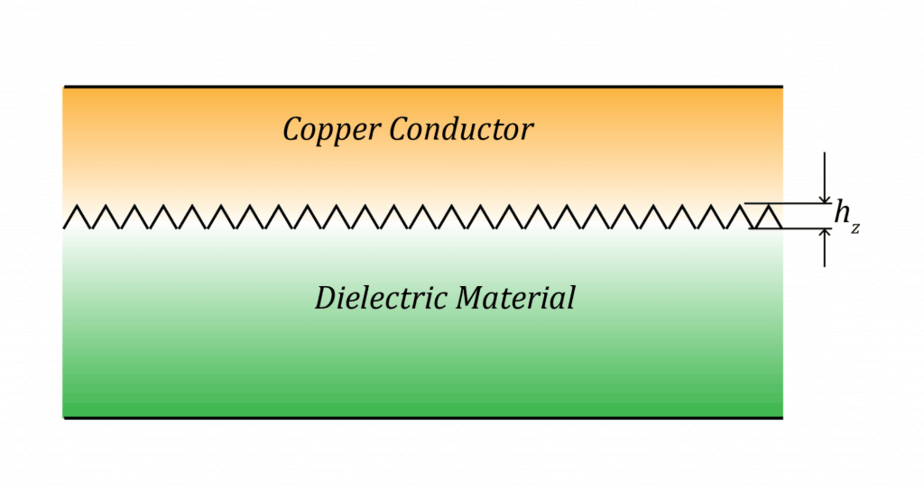
Where:
hz = Peak to peak height of teeth
hz is a measure of surface roughness.
Typically, hz varies from one foil type to another and the typical values are:

If the roughness hz is smaller than the skin depth (which will be the case at very high frequencies), this will cause additional conductor losses. We experimentally observed this increase by making test circuit boards with different foils having different hz.
We found that losses in the case of VLF foil are lower than in the case of the usual HTE foil. For RF/microwave boards at frequencies greater than 1GHz, these conductor losses due to roughness can become significant over long signal lines.

At low frequencies, it will still be:
![]()
Use the higher of the equations above for R.
At high frequencies:
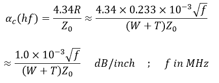
If f were in GHz and W and T in mils, we would get:

Let’s calculate it for a 5-mil, 1oz, 50-ohm and for a 4-mil, 0.5-oz, and 50-ohm line:

The important point to note is that at frequencies greater than 50MHz, conductor loss is proportional to the square root of the frequency:

It is not easy to predict the additional loss due to copper roughness – simple formulae do not exist.
Dielectric loss in a PCB transmission line
As was mentioned earlier, this is the dielectric loss in units of dB per unit length in a transmission line:
![]()
Where:
G = Conductance pul of the dielectric material
Z0 = Impedance of the transmission line is about ≈√L/C
Two properties characterize the PCB dielectric materials:
1. Dielectric constant – Dk or Er – also called relative permittivity.
2. Dissipation factor – Df – also called tanδ.
The board material manufacturers publish the values of Er and Df. We will now find the relation between G and Er, Df.

High-Speed PCB Design Guide
8 Chapters - 115 Pages - 150 Minute ReadWhat's Inside:
- Explanations of signal integrity issues
- Understanding transmission lines and controlled impedance
- Selection process of high-speed PCB materials
- High-speed layout guidelines
Download Now
Loss tangent/dissipation factor of a dielectric
We can model a dielectric layer between two conductors as a conductance G in parallel with a capacitance C:
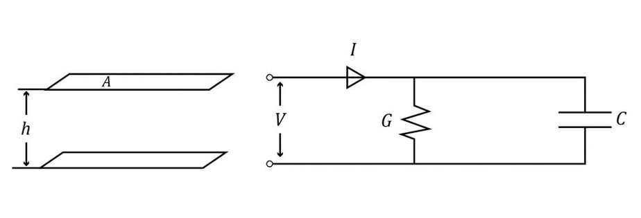
The AC voltage and current of frequency across this conductor is:

IG is the current through G and IC is the current through the capacitor.

tanδ is also called as dissipation factor Df ≡ tanδ.
If σ is the effective conductivity of the dielectric material, then:
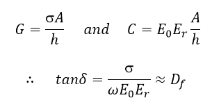
It has been experimentally observed that tanδ or Df varies very little with frequency and may be considered as a value independent of the frequency for all practical purposes:

The above equation indicates that conductivity σ and thus the conductance G of the dielectric increases with the frequency. This is something you can expect as the greater the frequency, the greater the dissipation of the heat in mechanical motion of dielectric dipoles in their effort to align with the alternating electric field across the dielectric. (We call it ‘damping of the vibrating dipole moments’.)
We now have:
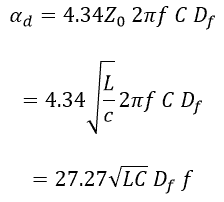
Recall that √LC gives the propagation delay per unit length – Pd – of the transmission line.
![]()
Now we have:

Therefore, we get:
![]()
We see from above that the dielectric loss is proportional to the frequency.
To get some idea of its magnitude, let’s consider the PCB materials Isola 370HR and I-Speed and I-Meta:

Total insertion loss in a PCB transmission line
It is the sum of conductor loss – ‘alfa’ C – and the dielectric loss: ‘alfa’ d.

We measure the value of the loss. (It is not easy to measure the conductor and dielectric losses separately.)
If we measure the insertion loss for sinusoidal signals at varying frequencies – say from 1 GHz to 10 GHz – we can use the above equation to separate the two types of losses:

If we now plot ‘alfa’ ins / √f vs √f, we expect a linear plot, from which we can determine A1 and A2.
At high-speed or high-frequency, we can’t ignore the transmission line effects. The losses in the PCB trace are dependent on the frequency, the dielectric constant (Dk), and the loss factor (Df). The losses will be higher at high frequencies, higher Dk value, and higher Df value. The roughness of the copper surface also increases the losses.
About the author: Atar Mittal is the Director and General Manager of design and assembly division at Sierra Circuits. He is responsible for the design and development of strategies and process automation tools for complex printed circuit boards and assemblies. Atar is also currently engaged in the development of productivity tools for electronics designers that would have a tremendous impact on shortening the development time.


