Contents

On-demand webinar
How Good is My Shield? An Introduction to Transfer Impedance and Shielding Effectiveness
by Karen Burnham
High density interconnect (HDI) technology is far more than the miniaturization of circuit design. It represents a significant breakthrough in our industry.
As Happy Holden, author of The HDI Handbook puts it, HDI breaks the traditional method of doing “the same things in the same ways, only smaller.” HDI advances have not only yielded improvements in the size and geometry of component attachment, but have also altered the electrical properties of the devices themselves, leading to lower power consumption and higher performance.
Implementing HDI at modern levels involved making changes in materials, imaging, assembly, testing, and design. This article examines those changes and takes a look at what we might see in the near future, as HDI continues to change the way we look at complex, compact circuits and the devices they make possible.
HDI PCB: An Overview
The twin forces of increasing functionality and decreasing package size have historically worked together to drive the development of HDI. Adding new features and capabilities to electronic products called for additional components and circuitry, but market demands, whether for consumer or commercial electronics, required increasingly smaller footprints and lower power consumption (typically measured in terms of battery life).
HDI began by solving the problem of how to mount components more efficiently. As the distance between devices shrank, engineers noticed a relationship between the rise time for inter-device signals and overall package size.
Reducing trace distance (the space from one device to the next) shortened the time required for inter-device voltages to reach the required level, both because the distance was lower and also because the corresponding capacitance was less. This contributed to the increased performance from products designed using developing HDI technologies.
One crucial technical advance that made HDI possible is the microvia, a new way of connecting components on a circuit board. Traditional printed circuit board (PCB) technology, from the late 1940s through the 1980s, relied on photo-etched traces between discrete components, often using mounting holes that passed completely through the PCB for ease of manufacture (such as with wave-soldering equipment).
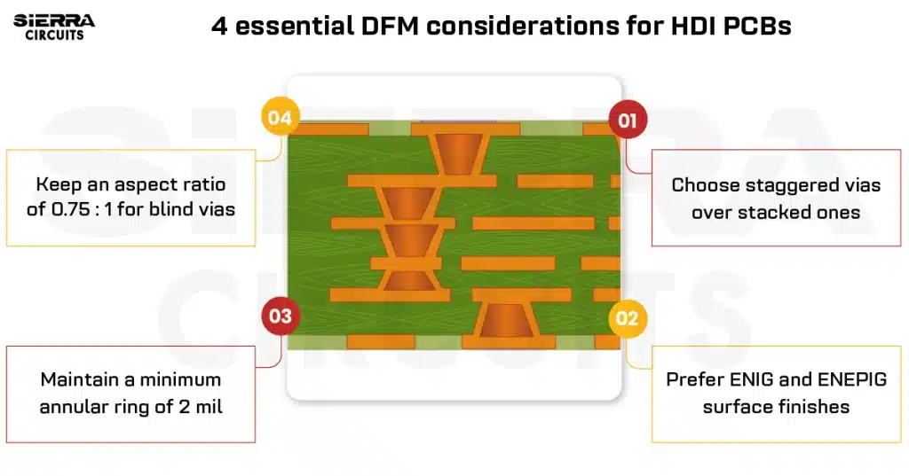
Beginning in the late 1990s, the microvia—a circuit path with significantly lower depth-to-diameter aspect ratios than the earlier through-hole vias—saw intense testing for performance and reliability. With aspect ratios of less than 1:1 (compared with through-hole vias with aspect ratios ranging from 6:1 to 20:1), these new, thin microvias performed with many times the thermal cycle life of their predecessors.
Originally, microvias and the HDI printed circuit boards they made possible were based around the then-new surface-mount device (SMD) technology, in which discrete components were soldered to the top layer of a PCB rather than passing through multiple layers. However, as functional complexity continued to grow, it became necessary to develop multilayer mounting and design techniques.
Early benchmarks determined that, compared to a controlled-impedance 12-layer through-hole design, an 8-layer HDI multilayer reduced the area of the PCB by 40%, as well as requiring four fewer layers. This reduced cost and at the same time made smaller products possible.
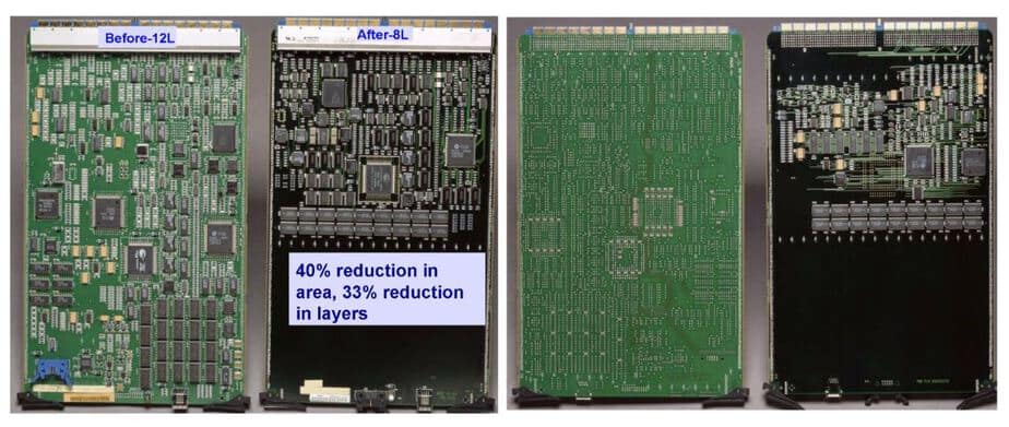
The multilayer/microvia approach involved changes in all stages of the PCB manufacturing process, but especially in components and design:
Components: Component design saw continued increase in complexity and reduction in size, consistent with Moore’s Law, which states that device density doubles roughly every 19 months. The increase in device density meant the creation of smaller devices with greater functionality capabilities, which significantly changed the requirements for PCB design.
Smaller devices made it possible to fit more on a single PCB; additionally, these devices often had more connections, which had to be accounted for on the PCB.
Design: PCB design, both rigid and flexible, had to adapt to successive developments in surface-mounted device (SMD) construction. Traditional PCBs could no longer keep up with the demands of these more modern, complex devices.
Devices had more traces with finer pitch, requiring PCB designs that addressed the reduced distances as well as the need to connect with multiple layers with the constraints of an SMD-based design.
Manufacturing: Just as the old-school through-hole design had to be phased out to deal with SMD components, its manufacturing process, using wave-soldering equipment, was also no longer applicable to modern IC packaging. Thermal adhesives, which bond the SMD component to the PCB, replaced the traditional technique of soldering pins from below.
Why HDI?
HDI offers a number of advantages in the areas of performance, package size, and overall weight. The combination of these makes HDI particularly attractive when applied to handheld, wearable and mobile electronics.
The primary motivation for HDI is simple: a larger number of transistors in a device provides more function and higher performance. In addition to increases in performance from using more powerful, more compact devices in a given product, the actual geometry of a high-density design can itself enhance performance.
Shorter traces (whether on-chip traces or the traces on the HDI board) reduce the amount of time it takes an electrical signal to travel between components. As another electrical advantage, smaller vias between devices (especially when coupled with smaller traces inside the devices) reduce the overall capacitance in the circuit, which reduces the rise time for the signal.
In addition, inductance is reduced with a high-density design, lowering the effect on neighboring leads and pins. This has been one case where HDI’s ability to place more transistors on a PCB has not only led to greater functionality on that device, but also to greater performance.
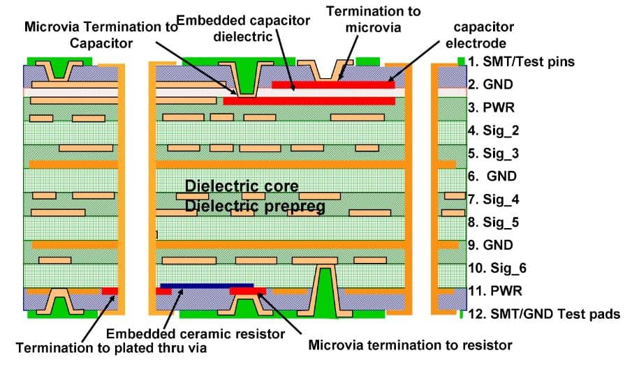
A side benefit to the reduction in overall capacitance has led to a reduction in required voltage in HDI devices. In turn, this drop in voltage not only means that smaller batteries are required, but also that heat generation is reduced, meaning heat dissipation is less problematic.
The elimination of large heat sinks or cooling fans in many HDI applications has contributed to the development of mobile and wearable electronics.
Finally, the development of design and manufacturing processes that focus on HDI layout and construction have led to a reduction in prototype development time and cost, and therefore can accelerate product introduction. This reduction in time-to-market (TTM) means a much greater profitability potential, as potential customers convert to actual customers more quickly.
Progression of Technologies
The technological advances that make modern HDI possible are essentially a dance between device makers and PCB designers, each of which offers new techniques that require, or sometimes permit, the other to move forward with device density.
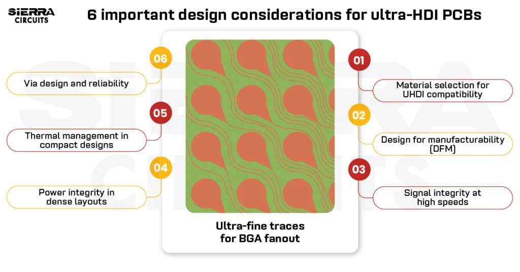
As integrated circuits became more powerful and smaller, the technology for mounting them to PCBs had to adapt to take full advantage of the newer devices. Early dense ICs included ball-grid array (BGA) devices, in which the entire underside of the device was available for connections, rather than packaging with pins along each side as in the dual-inline package (DIP) designs previously standard in IC construction.
BGA mounts, with their very short leads, provided an important step towards the reduction of inductance-related signal distortion that helped the overall performance of HDI designs. The primary negative with BGA devices was the initial cost of converting to machinery that performed the task of mounting the BGA to the PCB; the wave-solder machines which were the mainstay of through-mounted DIP assembly were incapable of the surface-mount assembly required by BGA devices.
Chip-scale packages (CSP) took the BGA principle to the next level. Originally called “chip-size packages,” CSP components were designed with the intention that the device would be no larger than the chip itself, with BGA-type leads on the bottom of the device.
The name change reflected the packaging needs, which initially defined CSP devices as being no more than 1.2 times the size of the chip on which the device was based. However, as semiconductor manufacturing techniques were refined (and as Moore’s Law continued to prove accurate), the chips themselves shrank but the package size itself remained constant. The definition of CSP changed to refer to devices with a mounting ball pitch of no more than 1mm.
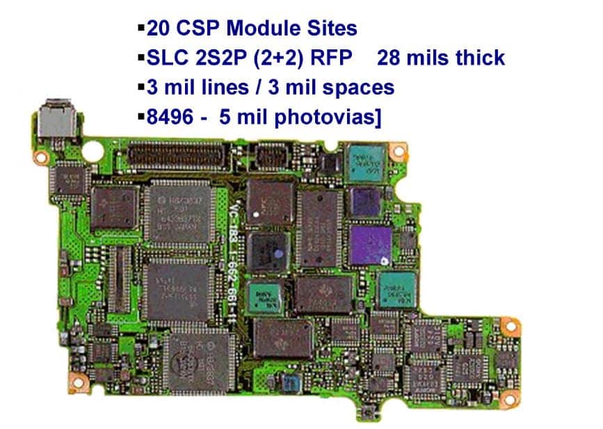
Direct chip attachment (DCA) continues the trend towards higher density by depositing the leads directly on the silicon, rather than using traces which connect the chip’s pads to the PCB.
This technique is also sometimes called “flip chip,” because the conductive pads are mounted on the wafer as the final stage of construction, then the devices are mounted upside-down on the PCB, typically using an underfill process to cover the sides of the die once in place.
From the PCB manufacturer’s standpoint, via-in-pad design works with DCA and CSP to ensure that these highly dense semiconductors have an efficient working environment once they are all in place in the eventual application.
Via-in-pad design places the via directly under the device’s pads, which is where the reduction in inductance, capacitance and heat generation makes a difference in the final application. Current via-in-pad design is capable of producing traces with a pitch of 0.75mm, and provides a flat surface for good device connectivity.
The Next Step: Sub-10nm Chips
The technological leapfrog between IC design and PCB technology has been responsible for today’s popular wearable and portable electronic devices, from miniature digital video cameras and laptops to smartphones and smart watches. The next advance in IC design is on the verge of reality, as the IBM/SUNY (State University of New York) Polytechnic 300mm research facility in Albany, NY unveiled the first working chip with 7nm transistors.
While sub-10nm design has been demonstrated experimentally for more than a decade, the IBM/SUNY chips, which use a silicon-germanium (SiGe) base, are the first large-scale demonstration of the technology for the production of ICs.
The significance of this development: IBM states that due to tight stacking, these 7nm chips achieve a surface area reduction of almost 50% compared to today’s chips. The two keys to this development are the use of extreme ultraviolet (EUV) light for photolithography, and the use of SiGe for the traces themselves.
Compared to the current lithographic standard, which is an argon-fluoride laser with a wavelength 193nm wide, EUV has a wavelength of only 13.5nm. Furthermore, standard silicon has been unable to carry enough current at 7nm, because there were not enough atoms in such a narrow channel for signal propagation. The addition of germanium increases electron mobility enough that the devices can function.
7nm chips are still at least two years away from entering the mainstream of manufacturing technology, but the added complexity and richness of products built with SiGe chips will be the next challenge for HDI circuit designers. The initial challenge will most likely be to design smaller PCBs to fit the significant reduction in device footprint, which will most likely require new developments in small-trace design and manufacture.
Eventually, as the reduction in device size has always followed with an increase in performance and complexity, these small-trace designs will be forced to contend with greater complexity and a higher number of interconnections, with the same or smaller footprint. The history of HDI shows that this balancing act—of matching advances in IC design with advances in PCB design and construction—promises exciting times ahead.
About Amit Bahl : Amit Bahl, widely recognized as the PCB Guy, earned his Bachelor of Science in Engineering from UCLA. He is currently the Chief Revenue Officer at Sierra Circuits, where he continues to lead efforts to simplify the PCB design journey and support designers and engineers in creating high-quality boards.


