


Contents

On-demand webinar
How Good is My Shield? An Introduction to Transfer Impedance and Shielding Effectiveness
by Karen Burnham
Embedded PCB components are passive devices fabricated within the PCB substrate using conductive and dielectric materials. This integration reduces parasitic effects, enhances heat dissipation, and improves overall circuit performance.
Highlights:
- Embedded components reduce parasitic effects, enhance signal integrity, and improve thermal management compared to conventional SMT components.
- Allocate dedicated internal layers for embedded parts to improve routing efficiency and minimize interference.
- Use thermal vias and copper pours to dissipate heat and prevent performance degradation.
- Understand the trade-offs between space utilization, parasitic effects, thermal management, and cost.
In this article, you will learn the key strategies for integrating embedded components in your PCB layouts.
Watch the full webinar here: Improving PCB performance with embedded resistors and capacitors
What are embedded PCB components?

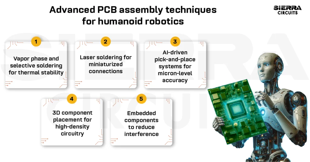
Embedded PCB components are electronic parts such as resistors, capacitors, inductors, and ICs that are directly integrated into PCB layers rather than on the surface. This advanced technique is used in advanced applications such as the assembly of humanoid robotics PCBs.
7 benefits of implementing embedded components
- Space efficient: Embedded passives occupy less space than SMT components, enabling compact designs.
- Reduced parasitic effects: These components minimize parasitic capacitance and inductance, improving signal integrity and offering better thermal management.
- Elimination of solder joints: Boards with embedded components do not require solder joints, reducing the risks of mechanical failure.
- Improved durability: Your PCB designs will be more resistant to shock, vibration, and temperature fluctuations, ensuring they perform well even in harsh environments.
- Ideal for high-density designs: These parts are perfect for HDI PCBs and miniaturized designs, helping you achieve the required form factor.
- Enhanced RF performance: The embedded resistors have been tested for RF characterization. For example, an attenuator tested up to 60 GHz shows excellent performance. Additionally, the impact of resistor material located beneath traces at frequencies up to 40–50 GHz showed only a minor signal loss due to the resistor material.
- Regulatory compliance: Embedded passives meet industry standards, with UL and IPC establishing specifications for resistors and capacitors. Products using these materials can achieve UL certification through standard testing.
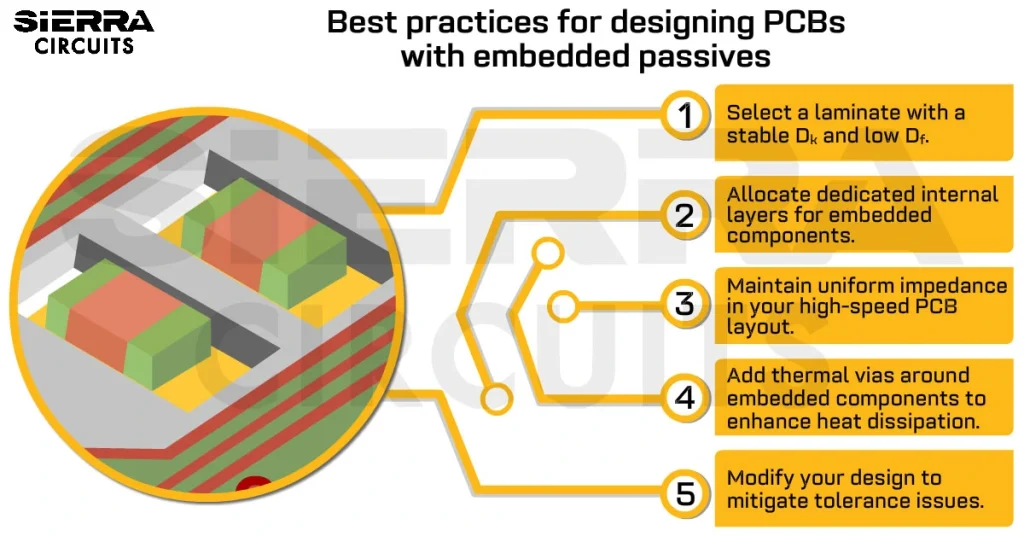
5 best practices for designing PCBs with embedded passives
To integrate embedded parts in your layout, you must create an additional layer specifically for these parts. This layer is called a window layer. All standard PCB layout tools, including Altium Designer, Cadence Allegro, and Zuken CADSTAR offer options to embed components.
Stick to these guidelines when designing printed boards with embedded parts:
1. Select a laminate with a stable Dk and low Df

- Pick materials with a stable dielectric constant over the operating temperature and frequency ranges.
- For high-frequency circuits, use materials with a Dk between 3.5 and 4.5 to balance performance and manufacturability.
- For RF PCB designs, use materials with a Dk of less than 3.0. Lower Dk values help reduce signal loss and improve overall signal integrity.
- Select materials with high thermal conductivity to enhance heat dissipation (greater than 0.5 Watts per meter-Kelvin).
2. Allocate dedicated internal layers for embedded components
Stack-up design plays an essential role in ensuring the reliability and performance of the overall prototype. By balancing layer distribution and optimizing shielding, you can minimize interference, improve signal integrity, and enhance overall manufacturability.
- Allocate specific internal layers for embedded resistors and capacitors to simplify routing and reduce the risk of interference.
- Ensure the stack-up is symmetrical to prevent warping. Balance the number of layers on both sides of the core for an even distribution of thermal and mechanical stresses during fabrication.
- Position embedded components as close as possible to the signal layers. This minimizes stubs and improves signal integrity.
- Include ground planes directly below the layers containing embedded passives. This helps reduce noise and enhance shielding. For flex PCB shielding methods, see best EMI and RF shielding methods for flex PCBs.
- Ensure the dielectric layers are thick enough, typically between 5 to 10 mil, to safely handle the operating voltages without compromising the electrical performance or safety.
- You don’t have to create a window layer to place resistors. Instead, you can directly place the resistors on the internal layer (as shown below). This eliminates the need for vias and does not add extra signal layers.

- For incorporating capacitors, create a window layer near the reference plane.

Download our eBook for more stack-up design guidelines.
PCB Stack-Up Design Guide
12 Chapters - 55 Pages - 60 Minute ReadWhat's Inside:
- Design guidelines for HDI, flex, and hybrid stack-ups
- Stack-up representation in fab drawing
- DFM checks for layer stacks
- Characteristics of high-speed materials
- Manufacturing tolerances
- PCB stack-up examples with illustrations
Download Now
3. Maintain uniform impedance in high-speed PCB layouts

To ensure consistent impedance in PCBs with embedded components, follow these practices:
- When designing traces, consider the copper thickness and adjust the trace width and spacing to achieve the target impedance. The thicker the copper, the lower the impedance.
- Implement transmission line stubs to achieve the desired impedance matching. Carefully adjust the stub length and position to achieve desired signal reflection characteristics and impedance alignment.
- Do not place embedded components beneath high-speed traces unless they are part of the impedance-matching network. This prevents unwanted signal disruptions or interference.
- Optimize the trace dimensions using impedance modeling tools.
- Perform time-domain reflectometry (TDR) measurements on PCB prototypes to verify impedance. This technique helps identify any inconsistencies in impedance across the PCB, ensuring the design performs as intended.
4. Add thermal vias around embedded parts to enhance heat dissipation

Since embedded components are enclosed within the PCB layers, efficient heat dissipation is essential to prevent thermal stress, which can lead to signal degradation.
- Position embedded passives away from heat-generating components like crystal oscillators and high-precision analog circuits.
- Incorporate sufficient ventilation to circulate air over the components to prevent overheating.
- Add thermal vias around and beneath embedded components to create efficient heat paths.
- Use large copper pours on internal layers to help distribute heat evenly across the printed board. Copper pours provide a path for heat to spread, reducing hot spots and improving overall thermal management.
- Connect embedded components to external heat sinks or thermal pads.
For more, see 12 PCB thermal management techniques to reduce heating.

5. Consider resistance variation and layer misregistration to avoid tolerance issues
Tolerance issues occur when the actual resistance value differs from the intended value due to manufacturing limitations. Factors like etching precision, feature size, and alignment during fabrication can cause these variations.
To address tolerance issues, artwork modifications are crucial. You need to consider two primary challenges:
- Resistance variation: This is influenced by the width and length of the etched features and the registration accuracy.
- Layer misregistration: During the two-step etching process, there may be slight misregistration between the first and second etches.
To overcome the above hurdles:
- Ensure your manufacturer is implementing techniques like laser direct imaging to achieve good registration, typically within a 1-mil placement tolerance.
- Design electrodes slightly larger than the resistor area to ensure the resistor remains fully within the electrode boundary and prevent deviations in resistance values.
- Aim for larger resistor dimensions wherever possible. Wider resistors (≥10–20 mil) reduce variability compared to narrow 5-mil-wide resistors.
At Sierra Circuits, we have automated scaling systems, laser direct imaging, and vision drilling to manufacture high-quality boards. Visit our rigid PCB manufacturing capabilities to learn more.
SMT components vs. embedded components
Here’s a quick comparison between SMT and embedded passives.

When deciding between SMT and embedded components, it ultimately depends on your application. If you are on a budget, SMT is the way to go. However, if the primary concern is having a compact design, thermal management, and reliability, embedded parts are worth considering despite their higher initial cost.
Download our design guide for DFA tips.

Design for Assembly Handbook
6 Chapters - 50 Pages - 70 Minute ReadWhat's Inside:
- Recommended layout for components
- Common PCB assembly defects
- Factors that impact the cost of the PCB assembly, including:
- Component packages
- Board assembly volumes
Download Now
4 factors to consider when choosing embedded resistors
1. Resistance and tolerance

The resistor’s base tolerance is typically around ±5%. Additional etching tolerances during manufacturing can increase this to 10–15%, resulting in an overall tolerance range of 15–20%.
The final tolerances depend on factors such as the resistor size, board material, and manufacturing process.
- Choose resistor values that maintain consistent impedance throughout the circuit. This is essential for achieving stable performance.
- Incorporate resistors with tighter tolerances, such as ±0.1% or better, into analog filters and oscillators. This improves accuracy and reduces variability in sensitive applications.
- Calculate the resistor dimensions using the formula R=(ρ×L)/(W×T).
Where,
-
- R is the desired resistance value (Ω)
- ρ is the resistivity of the resistive material (Ω·m)
- L is the length of the resistor (m)
- W is the width of the resistor (m)
- T is the thickness of the resistive layer (m)
- You can modify the length or width of the resistor to fine-tune its resistance value.
- When adjusting dimensions, confirm they align with your PCB manufacturer’s tolerances and fit within the available board space. This helps avoid design and production issues.
2. Power dissipation and current capacity
When a resistor is embedded in a PCB, the surrounding copper layers and prepreg material help dissipate heat, allowing it to handle higher power more efficiently.
Consider these guidelines to ensure power integrity:
- Calculate the power dissipation using the formula P=I2R.
- Ensure the resistor’s power rating is high enough to handle the calculated power dissipation. This step is crucial to avoid overheating and potential failure.
- Always select a resistor with a power rating that provides a safety margin above your calculated requirements. For safety, de-rate the resistor’s power capacity by at least 25%.
3. Temperature coefficient of resistance

TCR indicates how much a resistance value changes with temperature fluctuations. It’s measured in parts per million per degree Celsius. Choose resistors with a low TCR (below 100 ppm/°C) to minimize resistance variations caused by temperature changes. This ensures greater stability and accuracy in circuit performance.
4. Type of embedded resistors
When selecting embedded resistors, balancing performance, cost, and application-specific needs is important.
- For high-power or high-voltage designs, thick-film resistors may be the right choice.
- Pick thin-film resistors for precision and stability.
- Plated resistors are ideal for high-current and high-frequency applications.
Always match your choice with your circuit’s requirements.
4 tips to select embedded capacitors

- Always select a capacitor with a voltage rating 20–50% higher than the maximum expected voltage in your circuit. A capacitor’s voltage rating represents the maximum DC voltage it can handle without dielectric breakdown.
- Use ceramic capacitors in the range of 0.01 to 0.1 microFarads. These can stabilize voltage and filter out noise in power supply lines.
- For RF filters, select capacitance between 1 and 100 nanoFarads.
- For audio filters, pick capacitors in the range of 1 to 10 microFarads, as they are better suited for lower-frequency audio applications.
6 best strategies for effective decoupling with embedded capacitors

- Choose low ESR capacitors for high-frequency noise filtering.
- Position embedded capacitors directly adjacent to the power pins of the ICs to maximize decoupling efficiency.
- Add them in multiple PCB layers to target and filter a broader range of noise frequencies.
- Keep the traces between the embedded capacitors and the IC power pins as short as possible to reduce inductance and improve performance.
- Use solid and continuous power planes to provide a stable voltage reference and effectively distribute power throughout the circuit.
- Enhance the decoupling capacitor’s performance by combining embedded capacitors with discrete SMT capacitors.
Manufacturing considerations for embedded PCB components
1. Additional layer in the stack-up for embedded resistors

To embed resistors, a resistive layer is added to the entire layer. The etching process removes excess material.
Since the resistor material is extremely thin (1/2 oz), it can be incorporated into a signal layer without significantly increasing the thickness.
For example, a 10 Ω/square resistive material adds just about a micron in thickness, which is negligible. Even if an extra signal plane is required, it only adds the ½ oz. copper layer. For embedded capacitors, the overall thickness may decrease since power and ground planes can be placed closer together, reducing the required dielectric spacing.
You can use a signal layer for routing high-speed and placing an embedded resistor. The resistive layer is extremely thin, and the copper used is low-profile. Signal loss caused by the resistive layer is negligible (only fractions of decibels per inch).
This approach is widely used in products with PTFE-based materials, where high-speed signal traces and electromagnetic absorption applications are common.
For step-by-step fabrication process of embedded passives, see Ohmegaply and TCR materials with embedded passives technology in PCB manufacturing.
2. Drilling and microvia aspects
When drilling a pad on a layer with embedded resistors, ensure the resistors are offset from the pad. This reduces heat and mechanical stress on the resistive layer during the PCB drilling process.
Microvias can be used in layers with embedded resistors or capacitors without restrictions. However, clearance around microvias may need adjustments. Always consult the manufacturer for specific guidelines and best practices.
3. Manufacturing cost and turnaround time
Higher resistor density makes embedded resistor designs more cost-effective. For example, embedding resistors significantly reduces costs in MEMS microphones.
However, cost savings depend on the design and may not always be a one-to-one reduction. In many cases, the primary advantage isn’t cost but performance improvements and reduced printed board size.
Quick-turn manufacturing (1–3 days) is generally not feasible for embedded component designs. Expect an additional 3 days to standard turnaround times.
Fab notes for integrating embedded components
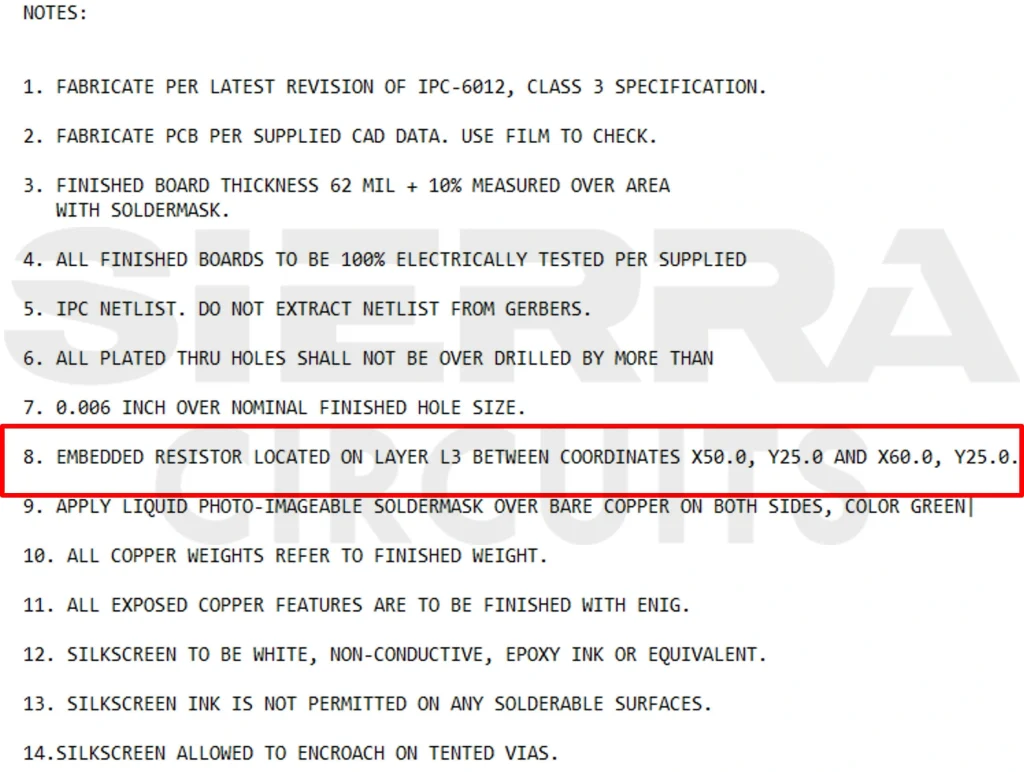
You must cover several essential details in your fabrication notes for a board with embedded passives. Let’s go over the key points:
- Indicate the layer and orientation of each embedded component.
- Add XY coordinates and component specifications.
- Provide precise dimensions and tolerances of cavities.
- Specify the depth of each cavity accurately.
- Define the shape of each cavity and any special features.
- Add the minimum clearance between the cavity walls and the embedded component to allow for assembly and manufacturing variations.
- Attach datasheets for all embedded components, including specifications, dimensions, and thermal characteristics.
Key takeaways:
- Integrating passive components into PCB layers enhances signal integrity and thermal management.
- Without solder joints, embedded components withstand shock, vibration, and temperature fluctuations better.
- SMT components are easier to modify and cost-effective, while embedded passives excel in compactness and efficiency.
- Choosing embedded resistors and capacitors requires careful consideration of resistance tolerance, power dissipation, TCR, and voltage ratings.
Embedded resistors and capacitors present a compelling alternative to traditional SMT components, offering enhanced reliability, thermal management, and space efficiency. However, their adoption requires careful consideration of cost, manufacturability, and design constraints.
By understanding the selection criteria, design strategies, and implementation best practices outlined in this blog, designers can effectively integrate embedded PCB components into their designs, improving overall circuit performance.
Have any design queries? Post them on our forum, SierraConnect. Our PCB experts will answer them.


Start the discussion at sierraconnect.protoexpress.com