


Contents

On-demand webinar
How Good is My Shield? An Introduction to Transfer Impedance and Shielding Effectiveness
by Karen Burnham
An ESD protection circuit safeguards sensitive PCB components from high voltage spikes caused by an electrostatic discharge event.
ESD occurs when a charged object comes in contact with an electronic device, releasing a sudden surge of electricity. This surge can damage low-voltage components such as microprocessors, FPGAs, memory chips, and analog ICs.
By implementing static discharge and TVS diodes, you can redirect harmful currents to the ground. Proper placement and selection of these diodes are crucial to mitigate risks and enhance the robustness of the PCB design.
Highlights:
- ESD diodes and TVS diodes clamp voltage spikes and redirect them to the ground.
- Selection and placement of the diodes play a crucial role in protecting your board from electrostatic discharge.
- IEC 61000-4-2 is a standard to evaluate the ESD immunity of electronic devices.
In this blog, you will learn the best practices for designing an ESD protection circuit.
What is an ESD protection circuit?
ESD protection circuits shield devices from electrostatic discharge, i.e., rapid transfer of charge between two objects of different electrostatic potentials. This discharge can occur when a person or object with a static charge comes in contact with sensitive electronic components, causing voltage spikes.
These voltage spikes can be suppressed using ESD protection circuits with electrostatic discharge diodes, transient voltage suppression (TVS) diodes, or metal oxide varistors (MOVs). These devices clamp surges to safe levels, preventing damage to ICs.

ESD diodes are also commonly used to avoid electrostatic events, particularly in high-speed circuits. TVS diodes are often placed across power and ground lines. MOVs can be used for bulk energy absorption.

Understanding ESD waveform characteristics
Static discharge event typically follows a specific waveform profile, consisting of a sharp initial peak current followed by a gradual decay.
The rise time is extremely fast, often on the order of nanoseconds, with a di/dt (rate of change of current) as high as 30 A/ns. As this surge of current travels through a PCB, parasitic inductances, particularly in traces and vias, can cause voltage spikes that amplify the effects of ESD.

For tips on minimizing parasitic capacitance, see how to reduce parasitic capacitance in PCB layout.
Why does your PCB need an ESD protection circuit?
When ESD occurs, heat builds up in the printed boards due to the voltage drop caused by the traces’ resistance. This localized heating can reach extreme levels, especially if the current pulse is strong. The temperature rise can:
- Melt thin traces, creating open or short circuits.
- Damage solder joints.
- Delaminate PCB layers, compromising structural integrity.
Due to their compact design and low operating voltages (often 3.3V or lower), ICs such as BGA and QFN packages are highly susceptible to static discharge. Discharge pulses can create unintended conduction paths within the IC die, causing failures. The high voltage can breach insulation layers, disrupting functionality, while the excessive heat generated by static discharge can damage internal structures.

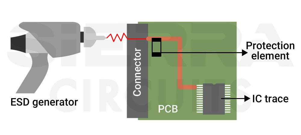
Connectors are hotspots for ESD events due to frequent interactions like plugging or unplugging cables. Static discharge can occur when you insert the cables into connectors, generating sparks and risking damage to nearby circuits.
Download our design guide to learn the best practices for incorporating connectors in PCBs.
Connector Design Guide
5 Chapters - 32 Pages - 50 Minute ReadWhat's Inside:
- Basics
- Terminology
- Selection and layout rules
- Testing
- Application-specific PCB connectors
Download Now
6 key layout tips to avoid electrostatic discharge in PCBs
1. Reduce the impedance in the ESD protection circuit
Parasitic inductance plays a critical role in the functionality of electrostatic diodes, particularly in high-speed circuits. This inductance comes from traces, vias, and component leads.
The parasitic effects add unwanted impedance to the current path. Increased impedance delays the ESD diode’s response, risking higher voltage spikes reaching the protected IC.

Consider the image above,
- LIN and LESD are the trace inductance connecting the ESD source and diode.
- LGND is the inductance between the diode and the ground.
- LIC is the trace inductance connecting the diode to the protected IC.
During the static discharge, both the ESD current and path impedance influence the voltage reaching the protected IC. The diode shunts current to the ground once the voltage exceeds a threshold, but parasitic inductance can delay this response.
Generally, LIN and LIC are part of the controlled impedance traces. You can guide the current through the diode by making LIC much larger than LIN.
Here are a few guidelines to make LIC greater than LIN:
- Reduce the length and increase the width of the traces between the ESD source and the diode.
- Place ICs far away from the diode.
- Avoid vias in the path between the ESD source and the diode. This can help lower the inductance, as vias introduce additional resistance and inductance.
If possible, eliminate LESD, representing a stub between the ESD source and the diode. Reduce LGND as much as possible by properly grounding the circuit.
Download our eBook to learn how to design a high-speed PCB with signal integrity.

High-Speed PCB Design Guide
8 Chapters - 115 Pages - 150 Minute ReadWhat's Inside:
- Explanations of signal integrity issues
- Understanding transmission lines and controlled impedance
- Selection process of high-speed PCB materials
- High-speed layout guidelines
Download Now
2. Place the diode close to the source
Proper ESD diode placement ensures faster response time, minimizing voltage spikes that could damage sensitive ICs.
Stick to these guidelines when placing safety diodes in your circuit:

- Place diode close to the potential ESD entry points, such as connectors, buttons, or exposed pads, is essential. This ensures the static energy is clamped before propagating further into the circuit. It also helps reduce EMI in your PCBs.
- Position the diode in parallel with the signal line. Connect one end of the diode to the signal path and the other to a ground plane.
- Ensure the diode has a low-impedance path to the ground plane, minimizing resistance and inductance for effective dissipation of ESD currents.
- Isolate signal lines around the diode to prevent interference.
For more component placement strategies, read component placement guidelines for PCB design and assembly.
3. Provide a low-inductance ground path in the ESD protection circuit
A low-inductance ground path helps to effectively dissipate the energy from an ESD surge, preventing harmful voltage spikes from reaching sensitive components.
To achieve a low-inductance ground connection, use multiple vias connecting the ESD diodes to the ground plane. The more vias you use, the lower the total inductance of the ground path.

The above image illustrates two grounding methods. In case 1, the vias connect the diode to the ground layer. To reduce LGND, you need to increase the number of vias connecting to the reference plane.
In case 2, the ESD diode ground is connected directly to the first-layer ground plane, maximizing the grounding efficiency.
Additionally, connect the ground plane directly to the metallic housing of the equipment when possible. This provides an additional dissipation path for the ESD energy, further reducing the potential for damage.
To learn more, see best PCB grounding techniques for high-power and HDI designs.
4. Keep the traces short and direct
When routing tracks to and from the ESD diode, keep them short and straight. This minimizes the impedance of the current path and reduces the overall voltage spike during the discharge event.
Avoid routing sensitive signal lines next to the ESD protection circuit, as this can lead to unwanted coupling and EMI due to the high dI/dt.

To learn how to design high-speed signal lines, see 10 layout tips for high-speed and high-current PCB traces.
5. Avoid vias in the transient suppression circuit

For optimal ESD protection, route traces directly from the discharge source to the diode without switching layers through a PCB via.
In the left image shown above, current flows to the diode before reaching the via, ensuring proper protection.
However, in the right image, the current splits between the protected IC and the ESD diode, reducing effectiveness. Avoid this since via inductance can divert current to the IC and increase voltage spikes, compromising protection.

6. Use filter components to reduce noise
In addition to diodes, other passive components like resistors and capacitors can help improve static discharge protection. Place a filter near the static discharge source to suppress high-frequency noise before it reaches sensitive areas of the PCB.
You can place these filters directly at the input/output connectors, where ESD events are most likely to occur.
Our engineering team recently encountered an issue where a USB connector was not detected during functional testing. This issue was raised because two unidirectional ESD protection diodes were connected to the USB’s differential pair.
The clamping voltages were too close to the operational voltage, causing unintended triggering. The issue was resolved by selecting diodes with a higher clamping voltage.
If you’re facing difficulty sourcing components for your PCB, check out our component sourcing and stocking services.
ESD diodes Vs. TVS diodes
One of the most effective ways to protect a system against electrostatic discharge is using an ESD diode or TVS diode. The table below summarizes the key differences between them:
Table 1: Difference between ESD diodes and TVS diodes
| Parameters | ESD diode | TVS diode |
|---|---|---|
| Purpose | Designed to protect sensitive electronic components from ESD. Intended to protect circuits from high-voltage, short-duration static events. | Built to protect against transient voltage spikes (high-energy voltage surges) caused by events like lightning strikes, power line crosses, or switching events in electrical circuits. They handle higher energy and longer-duration surges compared to ESD diodes. |
| Response time | Quick response time, typically in the nanosecond range, as they have to act against very short and fast pulses of static electricity. | Respond rapidly but are optimized for handling higher-energy transients over longer periods (microseconds to milliseconds). |
| Clamping voltage | Typically have a lower clamping voltage. This allows it to protect components from the low-voltage but high-speed static charges. | Have a higher clamping voltage, protecting against larger voltage surges without triggering for normal operating conditions. |
| Energy handling capability | Designed to handle lower amounts of energy because it protects against relatively small but high-speed electrostatic discharges. | Engineered to absorb higher energy levels, protecting circuits from larger voltage surges, such as those from lightning or other power line disturbances. |
| Applications | Commonly used in devices exposed to static electricity, such as computer peripherals, mobile devices, and sensitive semiconductor circuits. | Used in power supply lines, telecommunications equipment, automotive electronics, and systems where large voltage spikes are more common. |
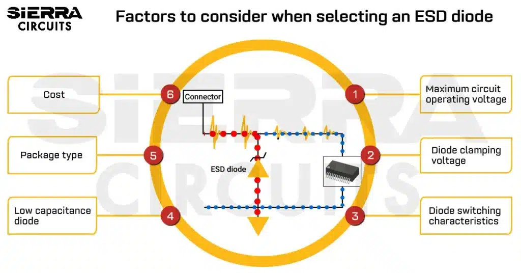
7 best practices for selecting ESD diodes

Here are the 7 key guidelines for selecting ESD diodes:
- Choose a diode with a clamping voltage slightly higher than the operating voltage but lower than the voltage rating of the protected components.
- Pick diodes with fast switching characteristics to quickly clamp any voltage spikes before they can damage sensitive components.
- Opt for the right diode for your application. Use unidirectional diodes for circuits with one-way signals, such as DC power lines or single-ended logic. For circuits with bidirectional signals, like data lines or AC signals, select bidirectional diodes to protect against both positive and negative ESD transients.
- For high-speed circuits, make sure the diode has low capacitance to minimize signal distortion. High capacitance slows down the circuit response, especially in data lines (USB, Ethernet, etc.).
- Select the right package type:
- SMTs are commonly selected for their compact size and compatibility with automated assembly.
- Through-hole diodes are used for higher power dissipation.
- Array packages have multiple protection diodes in a single package, which is suitable for multi-line protection.
- Ensure the ESD diode can handle continuous current without degradation. Check if continuous reverse current rating meets the requirements of your circuit, especially if it’s part of a power management or protection system.
- Balance performance and cost when selecting diodes. High-performance diodes provide better protection but can be expensive. Evaluate your component sensitivity and ESD risk—investing in a premium diode is often worthwhile for critical applications.
IEC 61000-4-2: Standard for electrostatic discharge testing
ESD testing ensures circuit reliability, identifying vulnerabilities and validating robustness against electrostatic events to reduce field failures and enhance long-term durability.
IEC 61000-4-2 is a widely recognized international standard that defines the requirements, methods, and severity levels for testing the susceptibility of electronic equipment to electrostatic discharge.
Adherence to this standard is essential for ensuring devices can withstand electrostatic discharge events without degradation or failure, making it critical for product reliability and safety. Compliance with IEC 61000-4-2 is often a prerequisite for product certification in international markets.
In addition to IEC 61000-4-2, here are the other standards that define guides for ESD testing:
- AEC-Q101 for automotive PCBs: Focuses on the reliability of discrete semiconductors in automotive applications. Covers ESD robustness under harsh operating conditions.
- ISO 10605 for vehicle systems: Addresses static discharge protection requirements specifically for vehicle electrical systems. Includes test conditions like temperature and humidity variations.
- ISO 9001 for manufacturing: Provides quality management standards, including ESD control measures in production processes.
- Military standards (MIL-STD-883): Defines testing methods for military-grade PCBs, focusing on extreme durability.
IEC 61000-4-2 testing procedure for an ESD protection circuit
Step 1: Place the device under test (DUT) on a non-conductive table positioned 0.8m above a ground reference plane.
Step 2: Position a horizontal coupling plane (HCP) and a vertical coupling plane (VCP) near the DUT to simulate indirect ESD effects. Connect a grounding cable from the DUT to the ground reference plane.
Step 3: Use the ESD simulator (gun) to replicate human body model (HBM) discharges with a 150pF capacitor and a 330Ω discharge resistor. This ensures the simulator complies with specified waveform characteristics (rise time, peak current, and energy content).
Step 4: Deliver discharges in two modes:
- Contact discharge: The gun makes direct contact with the DUT before discharging.
- Air discharge: The gun is brought close to the DUT, and discharge occurs through an air gap once the breakdown voltage is reached.
Step 5: Deliver ESD pulses to all key parts of the DUT. Include inputs, outputs, and exposed surfaces like connectors, buttons, and vents.
Step 6: Conduct the tests at specified standard levels (±2 kV, ±4 kV, ±6 kV, and ±8 kV), with custom levels up to ±15 kV based on application requirements.
Step 7: After the testing, evaluate the DUT’s performance using the following criteria:
- Class A: No degradation or loss of function; the device operates as intended.
- Class B: Temporary degradation or loss of function, but self-recovers without user intervention.
- Class C: Temporary loss of function requiring a reset or intervention.
- Class D: Permanent damage or loss of function requiring repair or replacement.
Key takeaways:
- An ESD protection circuit prevents high-voltage spikes from damaging sensitive components like microprocessors, memory chips, and analog ICs.
- Properly placed ESD and TVS diodes help redirect harmful currents to the ground, reducing the risk of PCB failure.
- High inductance in PCB traces and vias can delay diode response, increasing voltage spikes that damage components.
- Minimize trace length, avoid vias in protection paths, and ensure strong grounding to optimize protection.
- Standards like IEC 61000-4-2 define ESD test levels, ensuring devices meet reliability and safety requirements.
By comprehensively understanding ESD risks and implementing the right protection strategies, such as ESD or TVS diodes, designers can effectively reduce the risk of damage and ensure reliable performance in real-world conditions.
Need assistance in designing your high-speed boards? Post your queries on our forum, SierraConnect. Our PCB experts will answer them.


Start the discussion at sierraconnect.protoexpress.com