


Contents

On-demand webinar
How Good is My Shield? An Introduction to Transfer Impedance and Shielding Effectiveness
by Karen Burnham
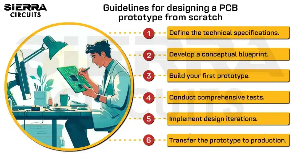
Designing a PCB prototype from scratch requires in-depth technical analysis and precise execution. This guide provides a comprehensive breakdown of the process, including every critical step from requirement gathering to final testing and regulatory compliance.
Highlights:
When creating a PCB prototype:
- Identify the end application, budget, and regulatory needs to set clear design expectations.
- Generate schematics, create PCB layouts, and perform simulations for design validation.
- Verify adherence to industry regulations like RoHS, FCC, and CE to meet industry standards.
- Use EVT (engineering validation test) samples for design verification before scaling production.
In this blog, you’ll learn the steps to create a successful PCB prototype, ensuring your design is ready for mass production.

1. Gather requirements from stakeholders
Defining project goals is the first step in creating a PCB prototype. It sets the foundation for the entire design process.
A thorough understanding of the requirements and an assessment of available technologies ensure your prototype aligns with its intended purpose while minimizing risks and inefficiencies.
1.1. Understand the project’s scope
This step involves engaging with stakeholders to clarify the scope and objectives of the project. This step ensures that all essential details about the application, operating conditions, and desired performance are documented and agreed upon.
Follow these steps to establish your project goals:
Step 1: Identify the end application
Clearly define the intent of your printed board. For example, is it for a consumer device, industrial equipment, or automotive system? The use case directly impacts the design complexity, power requirements, and environmental considerations.
Step 2: Define functional objectives
Outline the primary and secondary functionalities the printed board must support. This includes capabilities like data processing, communication protocols (e.g., Wi-Fi, Bluetooth), and user interface elements such as LED indicators or display screens.
Step 3: Determine performance metrics
Establish key performance indicators (KPIs), such as data throughput, processing speed, or energy efficiency. These metrics ensure the prototype meets expectations during PCB prototype testing and real-world deployment.
Step 4: Understand operational constraints
Investigate environmental factors like temperature, humidity, and exposure to vibrations. These constraints will shape decisions regarding material selection and component specifications.
Step 5: Establish budget and timeline
Practical considerations such as cost and time must align with the client’s goals. A detailed estimate for development and production phases helps manage expectations and allocate resources effectively.
Step 6: Address market and regulatory needs
Identify any region-specific certifications, such as FCC for the U.S. or CE for Europe, and ensure these requirements are incorporated into the design from the outset.
By consolidating all these details, you can create a requirement document that serves as a roadmap for the rest of the design process. A misstep here can lead to expensive redesigns or project delays.
1.2. Pick the best technology to build your PCB prototype
The research phase focuses on identifying and understanding the latest innovations, proven methodologies, and viable alternatives to ensure the prototype PCB design is cost-efficient and optimized for functionality. A few research steps are:
- Look for the availability and specifications of essential components such as microcontrollers, sensors, and connectors. For example, selecting a microcontroller with the right clock speed and I/O ports ensures optimal functionality without over-specifying or increasing prototype costs unnecessarily.
- Evaluate modern technologies that can add value to the design. For instance, advanced wireless modules (like BLE 5.2 or LoRa) or energy-efficient power management ICs can give the product a competitive edge.
- Investigate compatibility between selected components. For example, check if the microcontroller can interface seamlessly with external memory or communication modules.
- Study competitor products or similar applications to identify best practices, common pitfalls, and performance benchmarks. This comparative analysis helps refine design goals and aligns the project with industry standards.
- Assess manufacturing technologies such as high-density interconnect for compact designs or multi-layer boards for complex signal routing. The choice of PCB prototype manufacturing process can significantly impact design constraints and production costs.
- Explore EDA tools for schematic design, layout, and simulation. Tools like Altium Designer, Zuken CADSTAR, Siemens Xpedition, KiCad, and Cadence Allegro provide powerful features for designing and validating the PCB.

Key functionality of PCB layout design tools. - If the prototype is intended to scale to mass production, ensure the chosen technology supports efficient manufacturing processes. This includes the availability of components, repeatability of design, and assembly considerations.
- Assess the cost implications of various design choices, ensuring a balance between high performance and affordability. For example, selecting a slightly less advanced component could drastically reduce production costs while maintaining acceptable functionality. See how to reduce your PCB assembly cost for more details.
These steps not only minimize risks and inefficiencies but also help lay the groundwork for a successful PCB prototype.
2. Define the technical specifications of your prototype
This step ensures every aspect of the design is addressed, such as the functionality, power, regulatory compliance, and mechanical constraints. A well-defined specification minimizes ambiguities and sets clear expectations for design, development, and testing.
The hardware specification outlines the physical and functional aspects of the PCB. It provides the basis for component selection, layout decisions, and validation processes.
Follow these steps to clearly define the technical specs:
2.1. Outline the functional blocks and component requirements
- Specify the type and capacity of memory required, such as RAM, flash, or EEPROM. For instance, a device handling real-time data processing might require high-speed DDR4 memory, while a simpler IoT module may need minimal onboard flash for firmware storage.
- Choose a processor or microcontroller that matches the computational demands of the application. Factors such as clock speed, number of cores, and instruction sets must be considered. For example, a device with AI capabilities might need a specialized processor like an ARM Cortex-A series, while an embedded controller could use an ARM Cortex-M series.
- If the device includes a visual interface, define the display resolution, refresh rate, and type (LCD, OLED, etc.). Higher resolutions and larger displays increase power consumption and processing requirements, so these factors must be balanced.
- Specify insulation requirements to prevent current leakage and protect against short circuits. This is particularly critical in high-voltage or safety-critical applications.
2.2. Choose the right power source
- Define the power source. For battery-operated devices, consider battery type (e.g., Li-ion, NiMH), capacity, and expected runtime. For AC-powered devices, specify input voltage and required power adapters. Hybrid options, like battery backup for AC devices, might also be needed.
- Estimate and optimize the total power budget. This involves calculating the consumption of individual components and designing power management circuits. Power-hungry components like processors, wireless modules, and displays may require voltage regulators or efficient power supply ICs to maintain stable operation.
- Include requirements for power-saving modes, such as sleep or low-power states, to enhance energy efficiency in battery-powered applications.
2.3. Optimize your board for a specific environmental condition
- Define the operational temperature range (e.g., -40°C to 85°C for industrial applications or 0°C to 40°C for consumer devices). Component selection must align with these limits, and thermal management techniques such as heat sinks or thermal vias may be required.

Thermal vias for heat dissipation in prototype PCB design. - Specify the tolerance to humidity levels. Devices exposed to high-humidity environments might need conformal coatings to protect against moisture-induced corrosion or short circuits.
- For applications in automotive, aerospace, or industrial machinery, vibration resistance is critical. Mechanical reinforcements such as shock-absorbing mounts can help maintain integrity under continuous stress.
2.4. Comply with industry and regulatory standards
- Identify applicable safety certifications (e.g., UL, IEC 60950). These standards ensure the device is safe for end users, addressing concerns like electrical shock, fire hazards, and radiation.
- Ensure the design avoids restricted substances like lead, mercury, and cadmium, as per the RoHS (restriction of hazardous substances) directive. This is essential for market access in regions like the EU.
- Adhere to REACH (registration, evaluation, authorization, and restriction of chemicals) compliance by limiting harmful chemicals in materials and processes to promote environmental safety and user health.
- Obtain additional industry-specific certifications, such as MIL-STD-810 for mil-grade circuit boards.
- Follow applicable IPC standards such as IPC-6012 (rigid PCB performance), IPC-A-610 (assembly acceptability), IPC-2221 (design principles), etc.
2.5. Address the mechanical constraints and structural requirements
- Define the dimensions of the PCB to fit within the product’s enclosure. For compact devices like wearables, this might involve designing a high-density, multi-layer PCB to save space.
- Specify the weight limit if the product is portable. This is especially relevant for handheld or drone applications.
- Consider the form factor and mounting options. For example, irregular shapes might be needed for curved enclosures, while edge connectors or mounting holes are necessary for integration into larger systems.
- Include requirements for physical robustness, such as rigid-flex designs for foldable devices or reinforced boards for heavy-duty applications.
Defining these specifications at the outset ensures that all stakeholders—engineers, manufacturers, and quality assurance teams—have a clear, unified understanding of the design goals.
For high-speed design rules, download our design guide.

High-Speed PCB Design Guide
8 Chapters - 115 Pages - 150 Minute ReadWhat's Inside:
- Explanations of signal integrity issues
- Understanding transmission lines and controlled impedance
- Selection process of high-speed PCB materials
- High-speed layout guidelines
Download Now
3. Develop a conceptual blueprint for your prototype design
This phase focuses on conceptualizing and detailing the system. It also serves as the critical bridge between planning and implementation.
3.1. Create a system architecture document
The system architecture document (SAD) is a high-level representation of the entire system. It provides a comprehensive overview of how the sub-system modules interact with each other to achieve the desired functionality.
The document serves as the blueprint for the PCB prototype design and is crucial for streamlining communication across development teams.
It includes the failure mode assessment, which is a common phase throughout the design and implementation. It identifies potential failure points and risks, such as overheating, electromagnetic interference, or component failure.
A well-documented architecture helps minimize errors in subsequent stages and ensures the design meets system-wide requirements.
3.2. Build a detailed hardware design
The hardware detail design phase focuses on transforming the high-level architecture into a technically accurate and manufacturable PCB design. This involves specifying components, defining electrical connections, and planning the PCB layout in the following manner:
- Choose specific components (e.g., processors, power regulators, connectors) to meet performance, cost, and environmental constraints.
- Develop a high-level system diagram, specifying components. This includes analog and digital circuits, as well as mixed-signal design if required.
- Ensure proper connectors and pin assignments for power, communication, and signal lines. Misaligned or poorly planned connectors can lead to integration issues during prototype testing.
- Make sure that the hardware design aligns with the product’s physical enclosure. This involves verifying that the PCB dimensions, mounting holes, and connector locations match the mechanical design.
4. Translate the conceptualized data into a manufacturable PCB design
During design implementation, conceptual designs are translated into actionable outputs for manufacturing and assembly. This phase requires meticulous attention to detail and advanced expertise in electronics design and simulation tools to ensure the PCB meets both functional and manufacturability requirements.
Hardware development involves creating the schematics, layout, and simulations that transform the technical specifications into a functional PCB design.
The first version of the PCB is typically called proof of concept, and subsequent versions are named EVT (engineering validation test) and DVT (design validation test) samples.
4.1. Create schematics to represent electrical interconnections
Step 1: Draw the circuit using EDA tools
The schematic entry is the initial step in translating the design into a final output. You can use advanced EDA tools like Altium Designer, OrCAD, or KiCad to draw the circuit diagram. A few key considerations are:
- Proper hierarchical design to modularize complex circuits.
- Accurate pin mapping and library management for custom components.
- Cross-probing to verify connectivity between blocks and subsystems.
- Incorporation of design rules, such as voltage thresholds, current ratings, and net naming conventions.

For more, see how to draw and design a PCB schematic.
Step 2: Create a comprehensive BOM for all components
The bill of materials is a comprehensive list of all components in the schematic. A well-structured BOM includes:
- Component names, values, part numbers, tolerances, and package types.
- Manufacturer details, alternate part options, and sourcing information.
- Pricing, lead times, and availability to facilitate procurement.
To avoid stockouts, obsolescence, and last-minute redesigns, see the PCB procurement checklist for hardware engineers.

Use parametric filters in EDA tools to auto-generate BOMs with minimal manual intervention.

Step 3: Procure components from reliable suppliers
Procurement involves sourcing components from reliable vendors.
- Choose suppliers with traceability for components, ensuring compliance with industry standards (e.g., ROHS, REACH).
- Use vendor platforms like DigiKey or Mouser to find parts with minimal lead times.
- Plan for lifecycle management, ensuring components are not nearing obsolescence.

To eliminate potential supply chain disruptions, Sierra Circuits offers PCB component sourcing and stocking facility. We handle your components from quote to assembly.
Step 4: Run an analog simulation for circuit validation
Before moving to the layout, simulate the circuit to validate functionality. Analog simulation ensures key performance parameters (e.g., voltage levels, frequency response) meet requirements.
Tools like LTspice or Spice are used for:
- Validating signal integrity and gain in analog circuits.
- Analyzing transient, AC, and DC characteristics.
- Identifying potential design bottlenecks, such as excessive current draw or instability.
To learn more about circuit simulations, see how does circuit simulation work.
4.2. Transfer your schematics to a PCB layout file
Once the schematic is verified, the design is translated into a physical PCB layout. This step directly impacts the board’s manufacturability and electrical performance.
Step 1: Place components carefully on the board
Strategic component placement in PCB is a critical step.
- Group high-speed components to minimize trace lengths and reduce signal delay.
- Optimize the positioning of power components to enhance thermal dissipation and current flow.
- Ensure spacing meets DFM (design for manufacturability) and DRC (design rule check) guidelines.
Step 2: Build the PCB stack-up
Define the PCB stack-up, balancing signal integrity, cost, and design complexity.
- For high-speed designs, use multi-layer boards with dedicated ground and power planes to minimize crosstalk and impedance issues.

Segregate your circuits based on their functionalities in your prototype PCB design. - Specify core and prepreg thicknesses to control characteristic impedance for transmission lines.
- Switch to higher-quality PCB materials (e.g., FR4 to high-Tg laminate) for improved thermal or mechanical properties.
To learn how to choose the right materials for your prototype, see selecting PCB materials: electrical and manufacturing considerations.
Step 3: Route the signal traces
Routing is where signals are physically connected, following electrical and mechanical constraints.
- Maintain equal trace lengths for differential pairs (e.g., for USB, HDMI) to ensure proper signal timing.
- Use controlled impedance routing for high-frequency signals, requiring precise width and spacing calculations.

Abrupt changes in trace width lead to non-uniform impedance in PCB prototype design. - Optimize the thermal design by adding heat sinks or adjusting copper pours.
- Strengthen grounding mechanisms to prevent EMI.
- Ensure proper decoupling capacitor placement and routing of power lines to maintain power integrity.

Various placements of decoupling capacitors in the PDN design.
To learn advanced routing strategies, see 11 best high-speed design routing practices.
Step 4: Review the printed board for design validation
Perform an extensive and iterative review at each stage to ensure adherence to design rules, manufacturability, and signal requirements.
- Run electrical rule checks (ERC) and design rule checks (DRC).
- Conduct design reviews with cross-functional teams (mechanical, thermal, electrical) to validate design compatibility.
4.3. Perform a simulation to understand the signal and thermal behavior
1. Signal integrity
Signal integrity analysis ensures that high-speed signals (e.g., DDR, PCIe) experience minimal degradation.
- Use tools like HyperLynx or Ansys SIwave to identify reflections, crosstalk, and timing issues.
- Design termination strategies (e.g., series, parallel) to mitigate overshoot and ringing.
2. Thermal simulation
Thermal simulation predicts heat dissipation and temperature rise in power-hungry or compact designs.
- Simulate using tools like Ansys Icepak or FloTHERM.
- Add thermal vias, heat sinks, or thicker copper layers for improved PCB thermal management.

If any changes are needed based on the simulation result, then re-routing of certain traces will be done, and DRC will be re-run.
4.4. Run DFM and DFA checks
Apply design for manufacturability (DFM) and design for assembly (DFA) principles to simplify production and reduce assembly defects.
By applying these checks, potential production issues can be identified and addressed, improving overall yield and reliability.
For design for manufacturing rules, download our design guide.

Design for Manufacturing Handbook
11 Chapters - 96 Pages - 90 Minute ReadWhat's Inside:
- Annular rings: avoid drill breakouts
- Vias: optimize your design
- Trace width and space: follow the best practices
- Solder mask and silkscreen: get the must-knows
Download Now
4.5. Create fab notes and generate production files
PCB fab notes serve as a primary communication channel between the designers and fab houses. In your fab notes:
- Specify the appropriate substrate material (e.g., FR-4, Rogers) based on signal frequency and thermal requirements.
- Define tolerances for vias (plated vs. non-plated), copper thickness, and solder mask alignment.
- Mention the required PCB surface finish, such as ENIG (electroless nickel immersion gold) or HASL (hot air solder leveling), for surface finish quality.

After this, export the production files (IPC-2581/Gerber/ODB++) and submit them for prototype manufacturing. These files must be checked for accuracy using Gerber viewers like CAM350 to verify layers, alignment, and pad geometries.
4.6. Get your board fabricated and assembled
Once you submit your production files to your CM, your PCB prototype manufacturer will build your board.
PCB fabrication and assembly house will perform several tests before shipping the boards to the design team. The test may include a continuity test, flying probe test, in-circuit test, inspections, x-ray testing, AOI, and impedance verification.
After fabrication, the board will be populated with the designated components.
To reduce the turnaround time of your prototype, see how to get a quickturn PCB prototype in USA.
4.7. Initiate board bring-up to verify functionality
Board bring-up is the initial process of powering on and testing a newly assembled board to verify its basic functionality and identify any potential issues.
During this stage, you should:
- Verify fundamental hardware functionality by testing voltage levels, clock signals, and reset operations.
- Program the microcontroller or FPGA with firmware and confirm the basic operation.
- Test each module’s functionality (e.g., power regulation, communication protocols) individually before integrating.
- Utilize tools like oscilloscopes and logic analyzers to debug anomalies in power or data signals.
To learn how to get your prototype fabricated in 6 simple steps, see how to get your first PCB manufactured.
5. Conduct unit-level and integration tests
Unit-level and integration testing validate the functionality and interoperability of the board’s components and systems. These tests ensure the individual modules (unit-level) and their combined operation (integration) meet the design specifications and perform as intended.
Before testing begins, the respective team finalizes the software or firmware to ensure a stable and complete implementation.
Here’s how unit-level and integration tests are performed:
5.1. Outline the test protocol
The test protocol serves as the blueprint for conducting systematic and repeatable tests during unit-level and integration testing. It outlines the procedure, passing criteria, and tools necessary to evaluate the PCB’s functionality.
Step 1: Define test objectives
The protocol begins by specifying the objectives of the testing phase. For unit testing, the focus is on verifying individual components or subsystems (e.g., microcontrollers, power circuits, or sensors). Integration testing assesses how these units work together to achieve overall functionality.
Step 2: Identify test cases
Each test case addresses a specific performance parameter. For example:
-
- Voltage tests ensure power rails are delivering the correct voltage levels.
- Clock signal testing verifies stable oscillation frequencies.
- I/O validation confirms data integrity in communication protocols like I2C, SPI, or UART.
Test cases must also cover edge conditions and failure scenarios to ensure robustness.
Step 3: Specify the testing environment and tools
Mention the conditions under which tests should be conducted. This includes ambient temperature, humidity levels, and noise immunity to simulate real-world scenarios. Further, identify the tools and equipment needed for testing:
- Hardware: Oscilloscopes, multimeters, logic analyzers, and power analyzers for real-time measurements.
- Software: Automated testing frameworks, firmware debugging tools, and protocol analyzers for functional and performance checks.
Step 4: Define the pass/fail criteria
Clearly define the metrics for acceptance criteria. For instance:
- A voltage regulator output must be within ±5% of the target value.
- A microcontroller must respond to input signals within a specified time frame.
Step 5: Document the steps
Develop a logical sequence for executing tests, starting from the simplest (e.g., power-on tests) to the most complex (e.g., signal timing and data communication). This reduces the risk of cascading failures during integration testing.
5.2. Execute the unit-level and integration test protocol
The execution phase involves testing the prototype and assessing its performance at both unit and integration levels.
Step 1: Conduct unit-level testing for individual components
Test individual modules in isolation to ensure they function as expected. Examples include:
- Power subsystem testing: Verify if voltage regulators, power supplies, and battery management circuits operate within specified parameters.
- Signal integrity testing: Use oscilloscopes and signal analyzers to confirm undistorted signals between components.
- Sensor testing: Calibrate and check the response of sensors such as temperature, humidity, or pressure under controlled stimuli.
- Communication interfaces: Test protocols such as USB, Ethernet, or wireless modules to ensure reliable data transfer.
To learn more about wired and wireless communication interfaces, see a complete guide to PCB interfaces and communication protocols.
Step 2: Perform integration testing to evaluate module interactions
Assess how individual components interact as a system. Key aspects include:
- Inter-module communication: Ensure seamless data transfer between microcontrollers, memory, and peripheral devices.
- Timing and synchronization: Verify that clock signals and timing-critical operations align correctly across modules.
- Power load testing: Observe the system’s response to peak and idle power loads, ensuring stability across the entire board.
Step 3: Carry out debugging and iterative testing to identify faults
If anomalies are detected, use debugging tools such as in-circuit debuggers (ICDs) or JTAG interfaces. Make the desired corrections by rectifying hardware (e.g., replacing faulty components) or software (e.g., modifying firmware or driver code).
Conduct regression testing to ensure design updates do not introduce new issues while preserving validated features. It involves re-simulating and re-running tests to verify component and system functionality, ensuring design integrity and a reliable prototype.
5.3. Generate a test report
The test report is a formal record of the testing process, results, observations, and recommendations.
When creating the test report:
- Summarize the outcomes of all test cases, clearly indicating whether each test passed or failed.
- For failed tests, include details on the nature of the failure and its impact on functionality.
- Record critical data points, such as:
- Voltage and current measurements
- Timing diagrams for signal communication
- Response times for sensors or processors
- System behavior under edge-case conditions
- Provide an analysis identifying the root cause of any failures. This could involve design flaws, component defects, or environmental influences.
- Outline the steps taken to resolve detected issues, including hardware changes, software updates, or procedural improvements.
- Document compliance with the specifications defined in the design phase, such as power consumption limits, operating temperature ranges, or adherence to communication standards.
- Suggest improvements for future iterations, such as alternative components, layout adjustments, or enhancements to testing protocols.
- Present the report in a structured format with sections for test protocol, execution details, results, and conclusions. Include graphs, tables, and visuals for clarity.
These testing phases ensure the PCB prototype operates as intended and identify potential issues early, reducing risks and costs in later stages.
6. Refine the prototype by implementing design iterations
PCB design iteration is the process of refining the design based on test results.
Iterations are often necessary to address unforeseen challenges and fine-tune the design before mass production. This can involve multiple cycles of design, testing, and improvement.

In PCB prototyping, 2-3 iteration cycles are generally considered ideal for achieving a reliable and well-refined design.
If the process requires more cycles, it may indicate deeper design issues that need to be addressed, such as flaws in initial planning, component selection, or layout optimization.
7. Execute final functional testing
After refining your PCB prototype design, the next steps involve rigorous testing and validation. The complete board is evaluated under real-world operating conditions.
This ensures that the PCB meets its functional, electrical, safety, regulatory, and environmental specifications before scaling to production.
8. Perform EMC and safety tests
This stage focuses on validating the board’s electrical characteristics and ensuring compliance with industry safety standards to protect the end users from potential hazards.
8.1. Test the board for electromagnetic compatibility
Electromagnetic compatibility ensures the PCB operates within acceptable EMI limits. To ensure EMC, you need to perform the following tests:
- Emission test: Test radiated and conducted emissions using spectrum analyzers and near-field probes. Ensure compliance with relevant standards (e.g., CISPR 32 for emissions).
- Immunity test: Expose the PCB to radiated and conducted EM fields to verify its immunity. Tests include EFT (electrical fast transient), ESD (electrostatic discharge), and surge tests.
Address EMI issues using techniques such as adding optimized ground planes or implementing shielding enclosures.
9 key design considerations for EMC
To pass EMC testing, you must incorporate the following strategies during the design phase:
- Use a low-impedance ground plane to reduce noise and provide a stable reference for signal integrity.
- Minimize loop areas in signal traces to reduce radiation. Avoid routing high-speed signals near board edges and maintain controlled impedance for differential pairs.
- Add decoupling capacitors close to IC power pins to suppress high-frequency noise. EMI filters (e.g., LC filters) can be added at power entry points.

Power rail noise is reduced by placing the decoupling capacitors close to the IC power pins. - Use metal shielding cans over sensitive components or high-frequency circuits to confine radiated emissions.

Add shielding to the prototype PCB design to protect the circuit from EM radiation. - Utilize a multi-layer PCB with dedicated power and ground planes. Proper stack-up ensures effective electromagnetic shielding and minimizes crosstalk.
- Adhere to EMC regulatory standards to ensure the PCB design meets regional and industry-specific requirements. A few standards are:
- FCC Part 15 (USA): Governs radiated and conducted emissions.
- CISPR 22/32 (International): Specifies limits for IT equipment.
- IEC 61000-4-x: Defines immunity requirements for various disturbances.
- Place ESD (electrostatic discharge) suppressors or TVS (transient voltage suppressor) diodes at external interfaces. Design proper grounding paths for discharging static energy safely.
- Minimize clock trace lengths and use controlled impedance to prevent radiated emissions. Add series resistors for clock signal termination.
- Conduct pre-compliance testing before submitting prototypes to certified EMC labs. Tools include:
- Spectrum analyzers: Detect emissions across a range of frequencies.
- Near-field probes: Identify areas of high radiation on the PCB for optimization.
- ESD simulators: Test susceptibility to electrostatic discharge at key points on the PCB.
For more tips on how to mitigate EMI, see 7 tips and PCB design guidelines for EMI and EMC.
8.2. Ensure compliance with general safety tests
General safety tests ensure the PCB is safe for the end user.
Types of general safety tests include:
- Dielectric withstand test: Verify insulation strength by applying high voltage across critical points, ensuring no current leakage.
- Insulation resistance test: Calculate resistance between isolated circuits or components to detect potential short circuits or insulation degradation. High resistance indicates good insulation integrity.
- Leakage current test: Measure current leakage paths to confirm compliance with safety standards such as UL or IEC 60950, ensuring users are protected from electric shocks.
- Creepage and clearance check: Ensure adequate spacing between conductive paths to prevent arcing or short circuits.

Add adequate creepage and clearance distance in the prototype PCB design. - Overcurrent protection test: Validate that the PCB can handle fault conditions like short circuits or overcurrent without causing permanent damage. Overcurrent protection is often implemented through fuses, PTC thermistors, or current-limiting ICs.
- Temperature and thermal safety testing: Verify that the PCB does not overheat during operation and that the temperatures stay within safe limits. Components with excessive heat can degrade faster or pose a fire risk.
9. Obtain certifications for wireless regulatory compliance
Wireless-enabled PCBs must adhere to stringent regulations to ensure reliable operation and avoid interference. Compliance certification is mandatory for market entry and validates that the PCB design meets electromagnetic compatibility, spectrum allocation, and power output requirements.
Understanding these regulatory frameworks is crucial for PCB designers, as non-compliance can result in product recalls, fines, or the inability to market the device.
The FCC (Federal Communications Commission) governs wireless compliance for products sold in the United States.
Its regulations ensure that wireless devices do not interfere with other systems and operate safely within assigned frequency bands.
7 tips to ensure FCC compliance for your prototypes
- Comply with Part 15 of the FCC standard. This section covers unlicensed wireless devices, including Bluetooth, Wi-Fi, and Zigbee modules. Verify if the device operates within specified frequency ranges (e.g., 2.4 GHz ISM band) and meets maximum permissible radiated and conducted emissions levels.
Consider these subparts:
-
- Subpart B: Addresses unintentional radiators (e.g., clocks, oscillators).
- Subpart C: Focuses on intentional radiators like RF transmitters.
- If you’re working on an RF PCB design, ensure that the RF module operates within FCC-allocated bands and avoids restricted frequencies. For example, Wi-Fi operates in 2.4 GHz and 5 GHz, and these frequencies must comply with power output and emission regulations. Implement frequency-selective filters to limit spurious emissions and harmonic distortions.
- Regulate power output and optimize antenna design by adhering to FCC-mandated EIRP (effective isotropic radiated power) limits for different bands.
- Ensure that power amplifiers, antennas, and RF matching circuits meet these requirements.
- Use PCB trace antennas, chip antennas, or external antennas that align with FCC regulations. Ensure correct placement and isolation to avoid coupling or over-radiation.
- Meet FCC testing requirements stringently in your design. FCC certification involves lab tests for radiated emissions, conducted emissions, and spurious emissions. Designs must include proper test points for measuring signal integrity and output power. Pre-compliance testing can save PCB prototype costs and time by identifying potential failures early.
- Integrate pre-certified wireless modules properly without altering critical parameters such as antenna design, shielding, or RF traces. Modifications may void the module’s certification and require re-certification.
- Implement effective electromagnetic shielding and grounding to pass FCC compliance. Use Faraday cages, copper pours, and ground stitching vias.

Faraday cage shields sensitive circuitry in prototype PCB design from external EM radiation. - Include space in the PCB for an FCC ID label and additional marking if required. Documentation must detail the design’s RF characteristics, usage guidelines, and compliance reports.
Align your design with the applicable standard early to avoid expensive iterations and streamline the certification process for market-ready wireless products.
10. Carry out environmental testing of the PCB prototype design
Environmental testing ensures the PCB is robust and reliable under real-world conditions, particularly for applications where the PCB must operate under extreme or fluctuating environmental conditions.
10.1. Implement temperature and humidity tests
These tests evaluate the prototype’s performance under varying thermal and moisture conditions, which can significantly impact component functionality and structural integrity. The tests include:
- Thermal cycling: Test the PCB’s behavior under extreme temperatures, typically ranging from -40°C to +85°C or higher for industrial applications. Use environmental chambers to simulate temperature cycles.
- Humidity exposure: Simulate high-humidity conditions (e.g., 95% relative humidity) to evaluate susceptibility to moisture-induced failures like corrosion or short circuits.
- Condensation testing: Expose the board to temperature shifts that cause condensation and assess its ability to withstand moisture.
Moisture ingress or thermal cycling can cause delamination. Use high-Tg ( > 150°C) laminates to reduce risks. Incorporate moisture-resistant conformal coatings like acrylic, silicone, polyurethane, or gold-plated contacts in the design to minimize corrosion.
10.2. Run a vibration test to assess the board’s structural integrity
The vibration test evaluates the mechanical robustness of the PCB and its components under vibrational forces. The primary objectives of this test are:
- To validate the prototype’s ability to withstand operational or transport-related vibrations.
- To ensure that components, solder joints, and connectors remain intact and functional.
- To verify the mechanical integrity of the PCB’s layers, vias, and mounting mechanisms.
This test is essential for PCBs used in automotive, aerospace, industrial machinery, or any environment subject to physical shocks or vibrations.
3 vibration tests every PCB prototype must pass
- Sinusoidal vibration test: In this test, sinusoidal vibrations are applied to simulate repetitive mechanical forces the printed board might face in automotive or aerospace environments.
Sine wave vibration is applied across a range of frequencies (typically 5 Hz–2000 Hz) to identify resonant frequencies that may amplify vibrational stress. At these frequencies, components may experience fatigue or detachment.
You should ensure large components like transformers or inductors are securely fastened to avoid resonance effects.
- Random vibration test: This involves applying vibration across a spectrum of frequencies simultaneously, simulating real-world scenarios such as those experienced in vehicles.
Acceleration levels are measured in Grms (gravitational root mean square) with durations ranging from 8 to 24 hours.
The vibration levels are tailored to specific industries (e.g., MIL-STD-810 for military, IEC 61373 for railways).
- Shock testing: Simulate sudden impacts, such as drops or collisions, using a shock pulse with a high acceleration level (e.g., 50 g to 200 g). It assesses the board’s ability to survive abrupt mechanical forces.
Reinforce solder joints and consider using flexible PCB sections for shock-prone designs.
6 common PCB mechanical failures and how to prevent them
- Solder joint fatigue: Microcracks form at solder joints due to repetitive vibrational stress. Use solder materials with higher ductility, such as SAC305 or alloys.
- Component detachment: Large or heavy components are prone to lifting or snapping off.
- Reinforce these parts with adhesive or mechanical brackets.
- Implement underfill materials for components like BGAs to provide additional mechanical support.
- Place heavy components near the board’s center to reduce mechanical stress.
- Via cracking: High vibrations can crack vias, especially if the PCB undergoes thermal cycling as well. Use filled or plated-over vias for critical connections.
- Trace breakage: Flexural stress can cause traces to crack or peel. Incorporate tear-drop routing and avoid 90-degree bends in critical trace paths.
- PCB deformation: Large or flexible PCBs can deform under vibrational stress, leading to mechanical failures. Use circuit board stiffeners to reinforce flexible regions and prevent excessive bending or warping.

PCB deformation: Constraining force applied to one corner causes a twist. - Inadequate mounting stability: Poorly placed mounting holes or insufficient fixation can exacerbate vibrational stress across the PCB. Ensure proper placement and distribution of mounting holes to securely fix the board within the enclosure.
Adhere to standards such as MIL-STD-810 or ISO 16750-3 for vibration testing based on the industry application.
11. Use EVT samples for design validation
The EVT (engineering validation test) stage involves building and testing multiple prototypes to validate the design before moving to larger-scale production.
Step 1: Create sample boards for testing
Fabricate 5–25 PCBs to evaluate consistency across multiple units. This allows sufficient testing while controlling costs. EVT samples must be manufactured using production-level processes to closely mimic the final product. This includes:
- Using the same PCB stack-up, materials, and finishes (e.g., ENIG, HASL).
- Employing the final BOM components to validate sourcing and compatibility.
- Maintaining exact tolerances for vias, traces, and pads.
Step 2: Test the sample boards comprehensively
Repeat all functional, electrical, and environmental tests to ensure that the design performs consistently. Identify and rectify systemic flaws or manufacturing inconsistencies.
Step 3: Redesign if necessary
Use EVT results to address design issues, including performance bottlenecks, reliability concerns, or production challenges. Iterate the design before proceeding to the DVT (design validation test) stage.
12. Transfer the final design to production
After validation, the design is transferred to the supply chain for mass production. All necessary documentation, including work instructions, design files, checklists, incoming inspection guidelines, assembly testing methods, outgoing quality control procedures, and process checks, is handed over to the production house to ensure the manufacturing of a reliable PCB.
Key takeaways:
- Define product goals, operational requirements, and technical constraints before starting the PCB prototype design process.
- Evaluate components, manufacturing processes, and software tools to optimize performance and cost.
- Address functionality, power needs, environmental resilience, compliance, and mechanical constraints.
- Create a high-level design blueprint, identify potential failure points, and ensure seamless integration.
- Optimize manufacturability and assembly to minimize defects and improve production efficiency.
- Choose materials, define tolerances, and generate Gerber files for manufacturing.
- Conduct board bring-up, validate power and signals, and test functional modules to ensure proper operation.
- Validate individual components and system interoperability to ensure reliable PCB performance.
- Identify and resolve PCB design flaws in your prototype through iterative testing, debugging tools, and regression testing.
- Document results, failures, fixes, and compliance status to maintain transparency and traceability.
- Execute final functional testing to validate the fully assembled PCB under real-world conditions before mass production.
- Ensure compliance with EMC, environmental testing, and general safety standards for secure operation.
- Build and test prototypes to confirm design stability before scaling up production.
- Finalize documentation and ensure seamless handoff for mass manufacturing.
Designing a printed circuit board prototype from scratch is a meticulous process that requires careful planning, rigorous testing, and iterative refinement. A well-executed PCB prototyping process not only minimizes errors but also paves the way for a seamless transition to manufacturing, ultimately leading to a successful and market-ready product.
Have questions on your PCB prototype design? Post your queries on SierraConnect. Our PCB experts will answer them.

About Pooja Mitra : Pooja Mitra is an electronics and communication engineer. With an experience of over three years in the PCB industry, she creates industry-focused articles that help electrical and PCB layout engineers.


Start the discussion at sierraconnect.protoexpress.com