Contents

On-demand webinar
How Good is My Shield? An Introduction to Transfer Impedance and Shielding Effectiveness
by Karen Burnham
The autorouting plugin in KiCad automates the PCB routing process by creating optimized signal paths. It allows you to fine-tune the traces as per your requirements. This hybrid approach ensures layout efficiency and precision, making it ideal for complex designs.
KiCad users should be aware of this autorouting tool as it saves time, reduces errors, and enhances the quality of the layouts.
In this KiCad tutorial, you’ll learn how to set up FreeRouting and autoroute your PCB layout.
5 benefits of autorouting in KiCad
-
- Faster design process: Speeds up the design process by automating trace and via routing, saving design time.
- Error prevention: Follows predefined design rules and constraints, preventing issues like short circuits and missed connections.
- Optimized layouts: Utilizes advanced routing algorithms to route signals in dense or compact designs.
- Flexible design iterations: Allows manual re-routing, simplifying design modifications.
- Cost-efficient: Reduces the need for iterative prototypes, lowering development costs.
Prerequisite to install the FreeRouting plugin in KiCad
Before installing the FreeRouting plugin, install the Java runtime environment (JRE) in your PC.
Steps to install JRE on Windows
- Navigate to Java’s official website.
- Choose and download the JRE version that matches your Windows operating system and system architecture.
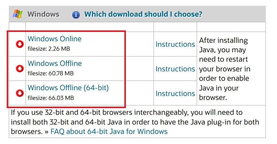
Steps to download JRE in the Windows operating system. - Run the installer once the download is complete, and follow the instructions.
Steps to install JRE on Linux
- Navigate to Java’s official website.
- Choose and download the JRE version that matches your Linux operating system and system architecture.
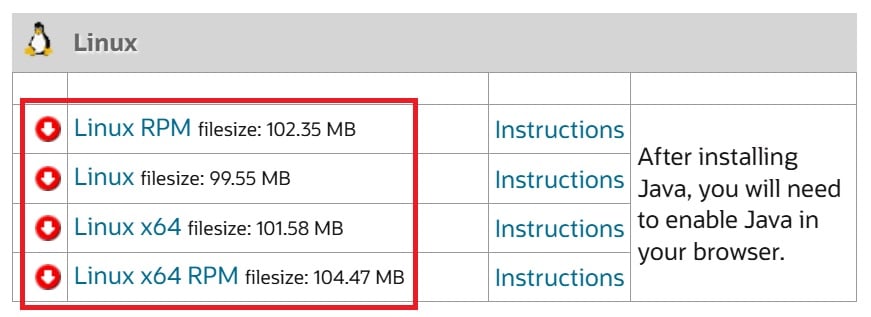
Steps to download JRE for the Linux operating system. - Change the directory where you want to install JRE.
- Open the jre-8uversion-linux-x64.tar.gz file and follow the instructions.
- Unpack the jre-8u431-linux file. The JRE will be installed in the selected directory.
After installing JRE, you can install the FreeRouting plugin.
How to install the autorouting plugin in KiCad
- Open KiCad and navigate to Plugin and Content Manager.
- In the search bar, type FreeRouting.
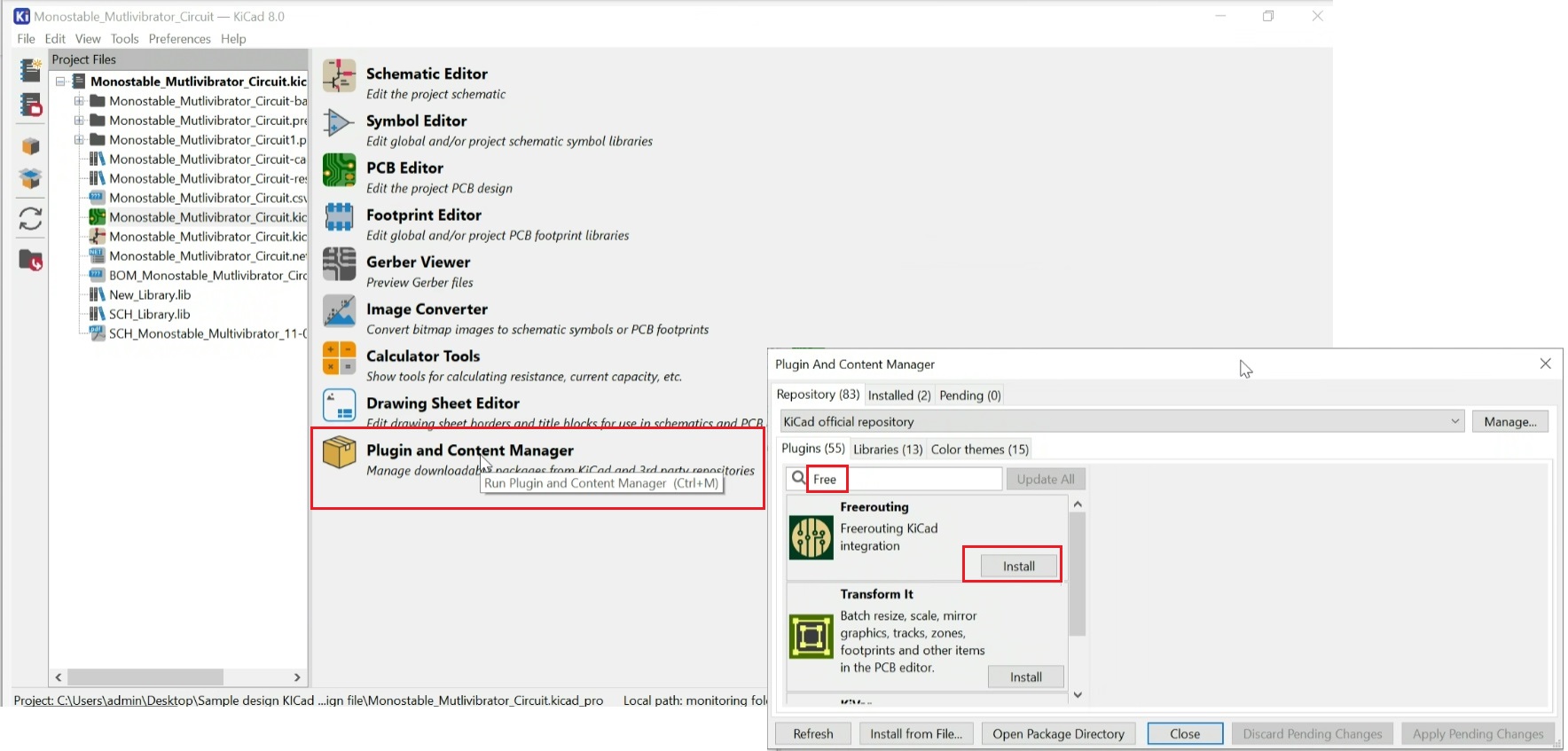
- Click on Install and Apply Pending Changes to complete the installation.
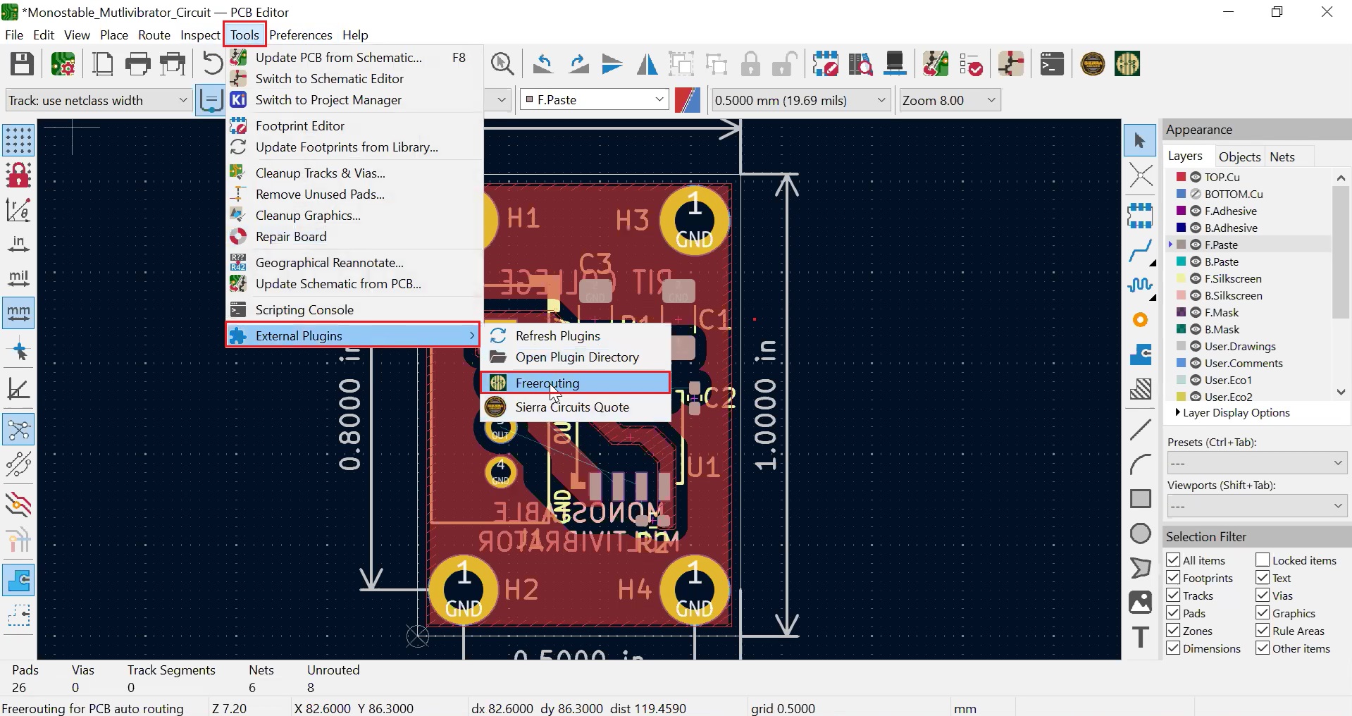
To access the FreeRouting plugin, go to Tools 🡪 External Plugins 🡪 FreeRouting in the PCB editor. Once installed, you can use the FreeRouting plugin to auto-route your designs.
For step-by-step guidelines on designing a PCB using KiCad, download our eBook.

KiCad Design Guide
10 Chapters - 161 Pages - 180 Minute ReadWhat's Inside:
- Creating a component symbol library
- Setting up board parameters and rules
- How to route differential pairs
- How to place of components
Download Now
Step-by-step procedure for autorouting in KiCad
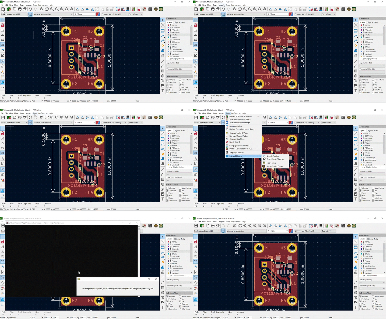
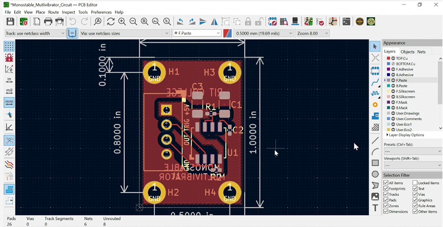
Step 1: Open a layout file with all the components placed.
Step 2: Go to Tools 🡪 External Plugins 🡪 FreeRouting to start the autorouting process.
The plugin automatically routes your PCB layout.
To learn how to manually route a layout, see our tutorial on how to route a PCB in KiCad.
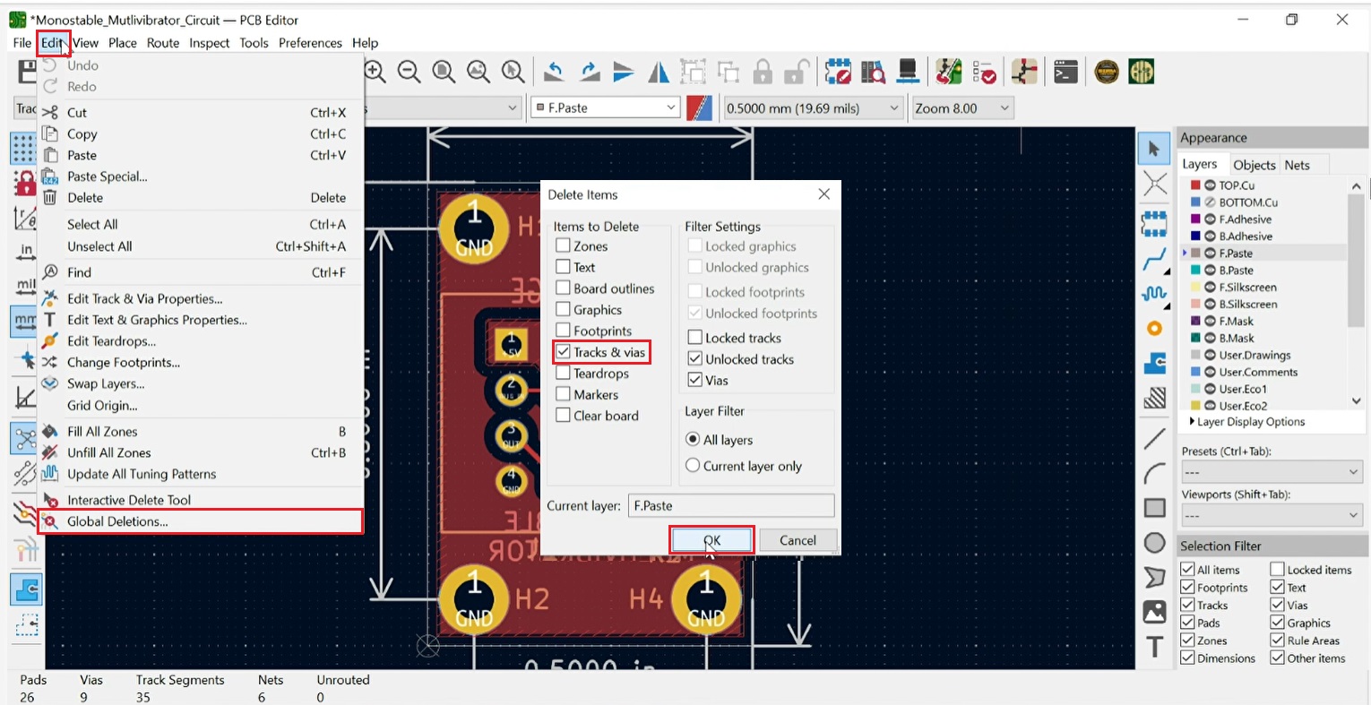
To delete all the autorouted tracks and vias, go to Edit 🡪 Global 🡪 Deletions. Check Track & Vias and hit OK.
After successfully autorouting your PCB layout, the next step is to secure a production quote.
To receive an instant cost estimate for your PCB design within the KiCad UI, install the KiCad Quote Plugin.
5 layout tips to optimize autorouting
To leverage the full potential of the FreeRouting plugin, consider these 6 practical tips:
- Define design rules and constraints: Before running the autorouter, set up the design rules for trace widths, clearance, and via sizes. These rules ensure the autorouter adheres to your specific design requirements and avoids rule violations.
- Efficiently place components: Auto-routing in KiCad results heavily depend on how components are arranged. Plan your layout strategically to minimize unnecessary routing complexity. For PCB component placement rules, see component placement guidelines for PCB design and assembly.
- Manually route critical traces: Manually route critical nets that require special attention. For instance, grounding paths should be short and wide. In addition to this, the number of vias in high-speed traces should be less.
- Use net classes to prioritize connections: Assign net classes to critical signals like high-speed or high-current traces. The autorouter will treat these nets with priority, ensuring better routing for sensitive signals.
- Review and fine-tune the autorouted layout: Review the results for potential improvements. Manual adjustments may still be needed for high-precision layouts, particularly in HDI or high-speed designs.
The FreeRouting plugin in KiCad is a valuable tool for streamlining the PCB design process. By automating the routing process and optimizing signal paths, it helps you save time and reduce errors. However, manual intervention is still necessary for critical signals and complex designs.
You can achieve high-quality PCB layouts by combining automated and manual routing techniques explained in this KiCad tutorial.
Need help in designing your PCBs? Post your queries on our forum, SierraConnect. Our PCB experts will answer them.













Start the discussion at sierraconnect.protoexpress.com