


Contents

On-demand webinar
How Good is My Shield? An Introduction to Transfer Impedance and Shielding Effectiveness
by Karen Burnham
Designing microwave boards involves meticulous selection of PCB materials, precise etching, and careful management of electromagnetic effects.
These boards are generally used in consumer devices like microwave ovens and high-bandwidth communication systems that operate at a very high frequency range (1 GHz to 30 GHz).


In this blog, you will learn the critical aspects of microwave PCB design, including material choices and the application of coplanar waveguides (CPW).
Highlights:
When designing microwave PCBs:
- Choose materials with a low Dk (2 to 4 at 10 GHz).
- Prefer PTFE, polyimide, and cyanate ester substrates.
- Select thinner substrates (10 to 20 mil) when operating at frequencies above 10 GHz.
- Utilize CPW designs for high-frequency applications.
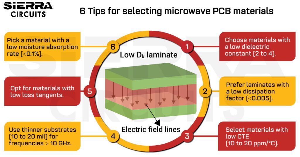
6 tips for selecting microwave PCB materials
When choosing a dielectric material for microwave boards, consider the following crucial properties of the dielectric material.
1. Choose materials with a low dielectric constant (2 to 4)
The dielectric constant measures a material’s ability to store electrical energy in an electric field.
Dk impacts the high-frequency operation, making it a primary concern for RF and microwave circuit boards. Therefore, select materials based on their performance in different frequency conditions.
The dielectric constant influences the speed at which electromagnetic signals propagate through the PCB substrate. Dk directly impacts signal delay and phase shift.

For microwave PCBs, choose materials with a relatively constant Dk across a wide range of frequencies. The lower the Dk value, the better, typically in the range of 2 to 4 at 10 GHz.
2. Prefer microwave PCB materials with a low dissipation factor (<0.005)
The dissipation factor (Df) is a vital parameter that indicates a material’s efficiency in converting electrical energy into heat. For microwave PCBs, lower Df values are preferred to minimize signal losses and ensure reliable performance.

For instance, RO3003 exhibits a Dk of 3 and a Df of 0.0013, whereas RO4350B has a Dk of 3.66 and a Df of 0.0031, making RO3003 the preferable choice due to its lower signal loss.
Choose a lower Df (<0.005) material for radio-frequency and microwave applications.
3. Select laminates with low CTE (10 to 20 ppm/°C) to ensure stable electrical properties
The coefficient of thermal expansion (CTE) measures the rate at which a material expands or contracts with temperature changes. In multilayer PCBs, CTE mismatch between layers can cause mechanical stress, warping, and potential reliability concerns.

Ideally, the CTE values of all materials used in a circuit board stack-up should be similar and closely match copper’s CTE. Significant differences in CTEs can cause thermal stress on the board at high frequencies.
For microwave boards, choose materials with low thermal expansion coefficients of 10 to 20 ppm/°C in the z-axis to maintain dimensional stability under varying temperatures.
RF & Microwave Design Guide
8 Chapters - 44 Pages - 60 Minute ReadWhat's Inside:
- Basics of RF and microwave board design
- Choosing RF materials
- Trace, grounding, via, and stack-up design
- Component selection and placement
- Testing and isolation requirements to avoid interference
Download Now
4. Use thinner substrates (10 to 20 mil) for operating frequencies above 10 GHz
The choice of substrate thickness depends on operating frequency, dielectric constant, and application requirements. It is typically in the range of 10 to 125 mil. The optimal substrate thickness can be chosen based on the specific design goals.
Always pick thinner substrates (10 to 20 mil) for frequencies above 10 GHz to avoid signal integrity issues.
5. Opt for materials with low loss tangents to minimize signal attenuation
Loss tangent (tan δ) is the signal loss caused by energy dissipation within the PCB substrate.
This dimensionless parameter is determined by the phase angle between the resistive and reactive components of a system. For instance, a capacitor should ideally exhibit only capacitance (C). However, real-world scenarios such as equivalent series resistance (ESR) contribute to the loss tangent, as depicted below.

Evaluating loss tangents is crucial in the material selection process for high-frequency applications. Materials with low loss tangents effectively minimize signal attenuation and distortion.
Typical values for loss tangent range from 0.0022 to 0.0095 within the 10-30 GHz frequency range.
6. Pick a material with a low moisture absorption rate (<0.1%)
Moisture absorption is a critical factor in microwave PCB materials, as moisture can significantly impact the dielectric properties and overall circuit performance.
In indoor settings, moisture absorption may not be a primary concern. However, in environments with high humidity, this characteristic becomes extremely important.
Water molecules have a high dielectric constant and can increase the dissipation factor of the laminate, leading to increased signal loss and degraded performance.
Microwave PCB materials are designed to have low moisture absorption rates to maintain stable dielectric properties and minimize the impact of environmental factors. Laminates with moisture absorption rates below 0.1% are suitable for microwave applications.
Materials such as PTFE and ceramic exhibit excellent moisture resistance. They are inherently hydrophobic and have minimal water absorption, making them ideal for applications exposed to humid environments.
Materials that meet all the above requirements include ceramic, fiberglass, and PTFE (Teflon). Among these, PTFE has the lowest dielectric constant (typically 2.6~2.7) and loss tangent (0.002). PTFE is the most widely used material for manufacturing microwave PCBs.
However, metallization is challenging for PTFE as the surface is smooth. To overcome this, at Sierra Circuits, we perform plasma and sodium etch (for thicker boards) treatments before plating to improve laminate metalization.
Sierra Circuits fabricates high-quality RF and microwave boards with operating frequencies ranging from 10 MHz to 30 GHz. See RF and microwave PCB manufacturing services to learn more.
Typical dielectric materials for microwave PCB designs
1. Laminate material
PTFE, polyimide, and cyanate ester (Dk = 2.5) are good substrate choices for microwave PCBs. Below are a few examples of such dielectric materials:
| Materials | Dielectric constant range | Composition | Key features | Variants |
|---|---|---|---|---|
| RO3000™ | 3.0 to 10.2 | PTFE filled with ceramic composite laminates |
|
RO3003™, RP3003G2™, RO3006™, RO3010™ |
| RO4000 | 2.55 to 6.15 | Hydrocarbon ceramic laminates |
|
RO4000 LoPro®, RO4003C, RO4350B, UL-94 V-0 flame retardant options available |
| Rogers TMM® | 3 to 13 | Advanced thermal microwave laminates |
|
TMM® 10, TMM® 10i, TMM® 13i, TMM® 3, TMM® 4 |

2. Bonding material
When assembling microwave PCBs, select bonding materials such as fluorinated ethylene propylene (FEP), ceramic-filled PTFE, and liquid crystal polymer (LCP). These materials offer low lamination and re-melt temperatures to maintain optimal performance.
3. Combination of materials
Opt for hybrid multi-layer circuit boards for critical, performance-driven applications. By combining different materials for various layers, such as using Rogers material for RF layers and FR4 for standard component layers, you can achieve the desired properties while optimizing costs.
This approach broadens the range of dielectric constants and thermal tolerances, ensuring efficient performance without compromising on budget constraints.
For more RF material selection tips, read how to pick RF PCB materials: 6 important factors to consider.
In addition to dielectric materials, the transmission line geometry is important in maintaining signal integrity in a microwave PCB.
Coplanar waveguides operate in a quasi-TEM mode, where a negligible portion of the EM field extends outward. This provides low dispersion and minimal dielectric loss, maintaining strong signal quality across a broad frequency range.
As an RF engineer, you should know about the coplanar waveguide structure, as it is the preferred trace geometry to route microwave signals with signal integrity.
How frequently do designers use coplanar waveguides
In our recent webinar, resolving common errors in RF PCB layout design, we surveyed 30 PCB designers, out of which 46.7% shared that they occasionally use coplanar waveguides in their microwave boards, while 33.3% have never incorporated them.

In the next section, we will explain the benefits of incorporating CPWs in your designs.
Why coplanar waveguides for microwave boards?
Various PCB transmission line options, such as microstrip, stripline, and CPW, are available, but their selection depends on factors like:
- The frequency band at which the board operates.
- Secondary considerations, like how the fabricated line aligns with the board’s design constraints.
On the higher end of the frequency spectrum, a coplanar waveguide is recommended.

CPWs are becoming more prominent in microwave PCB designs, especially for high-frequency applications, because it is compatible with millimeter-wave technology.
CPWs are primarily utilized for creating printed antennas, as they offer advantages over standard microstrips and discrete component-built antennas.

The central conductor serves as the feed for the antenna, where the input signal is applied. The ground planes provide a return path, which is crucial for maintaining signal integrity.
The signal line in CPWs terminates in a square or rectangular patch, enabling the antenna to direct signals perpendicular to the board surface. For tips on antenna placement, see antenna integration and RF design guidelines for 5G PCBs.
In contrast, traditional microstrip antennas often exhibit higher levels of cross-polarized radiation, resulting in reduced power output efficiency and increased thermal dissipation, which can accelerate board aging.
To learn how to design reliable transmission lines, download our eBook.

PCB Transmission Line eBook
5 Chapters - 20 Pages - 25 Minute ReadWhat's Inside:
- What is a PCB transmission line
- Signal speed and propagation delay
- Critical length, controlled impedance and rise/fall time
- Analyzing a PCB transmission line
Download Now
Benefits of incorporating CPW in high-frequency PCBs
Design and performance:
- The compact nature of CPW designs allows for much denser microwave circuits than traditional microstrip or stripline circuits.
- CPWs can be scaled to accommodate higher frequency applications, including millimeter-wave technology, which operates at frequencies above 30 GHz.
- The planar ground surrounding the signal lines significantly diminishes signal radiation, even for high-speed lines, making CPWs effective for separating high-speed signals from other signals.
- Coplanar waveguide improves signal integrity by offering higher gain compared to equivalent signal traces that use via techniques. This is achieved by reducing parasitic source inductance, as the closer proximity of the ground plane to the signal provides a more efficient return path.
- Coplanar waveguide design minimizes radiation loss and signal dispersion compared to microstrip lines.
Manufacturing:
- CPW designs are compatible with automated placement and soldering equipment used in PCB manufacturing. This compatibility ensures precise and efficient assembly processes, reducing potential errors.
- The design also supports automated soldering processes, ensuring reliable and consistent solder joints, which are essential for high-frequency performance and longevity.
- The uniplanar design allows for easy mounting of shunt components or active devices directly, without the need for via holes as required in microstrip lines.
- CPWs reduce the need for additional signal integrity structures such as via holes and wraparound edge plating.
- The impedance of CPWs is simpler to manage than that of microstrips, and it is determined primarily by the ratio of signal trace thickness to the total air gap distance (including the signal trace).
- CPW designs can reduce overall board costs by eliminating the need for backside processing, such as additional ground planes or via stitching.
To learn how to tackle microwave board design roadblocks, see microwave PCB design challenges and ways to overcome them.
Key takeaways:
- Prefer low Df (<0.005) microwave PCB materials to ensure signal integrity.
- Select materials with a low coefficient of thermal expansion (CTE) to prevent mechanical stress and warping in multilayer PCBs. Aim for an ideal CTE range of 10 to 20 ppm/°C for stability.
- Opt for microwave PCB materials with low loss tangents to reduce signal attenuation and distortion.
- Pick laminates with moisture absorption rates below 0.1% to maintain dielectric stability in humid environments.
- Consider Rogers materials, particularly the RO3000™ and RO4000 series, for their superior characteristics.
- Balance performance and cost by using hybrid materials, combining RF-optimized materials (like Rogers) with cost-effective ones (like FR4) for non-RF layers.
- Design printed antennas using CPWs to enhance signal integrity compared to traditional microstrip antennas.
Designing microwave PCBs requires a deep understanding of high-frequency behavior, precise material selection, and adherence to stringent design specifications. Using advanced materials like the RO3000™ and RO4000 series and incorporating coplanar waveguides, you can create high-performance boards for modern communication and radar systems.
Need help designing a microwave circuit board? Post your questions on our PCB forum, SierraConnect. Our design experts will resolve them.

About Pooja Mitra : Pooja Mitra is an electronics and communication engineer. With an experience of over three years in the PCB industry, she creates industry-focused articles that help electrical and PCB layout engineers.


How do variations in material Dk impact impedance matching in microwave layouts?
What’s your go-to method for optimizing CPW gap width to minimize signal radiation?
Variations in the dielectric constant (Dk) introduce minor discrepancies in impedance, which can cause small ripples in return loss plots. However, manufacturers account for this by incorporating a “guard band” into the specifications.
By adhering to nominal Dk values, you can typically maintain acceptable performance. While return loss may fluctuate within a range (e.g., ±10 dB), as long as the response remains below the target threshold (e.g., -20 dB), the design is considered effective.
Adjustments to the CPW gap width can be optimized using a vector network analyzer (VNA). The VNA provides precise insights into signal behavior, enabling effective identification and implementation of changes to minimize signal radiation.
What do you mean by “guard band”? Is this a slightly wider minimum width for trace and space? A thicker substrate or copper? A looser tolerance than they expect to achieve in practice? Design that still works fine at slightly higher or lower frequencies?