


Contents

On-demand webinar
How Good is My Shield? An Introduction to Transfer Impedance and Shielding Effectiveness
by Karen Burnham
KiCad is an open-source software that offers PCB designers and hobbyists a free yet powerful alternative to commercial EDA tools. It includes features for schematic capture, layout, and 3D visualization of your circuit boards.
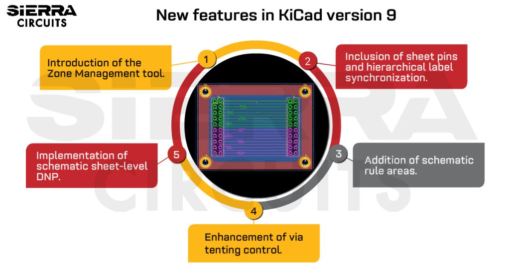
In KiCad version 9, you can expect significant upgrades, such as a new Zone Manager tool, enhanced net inspection, and schematic sheet-level DNP.
New version: KiCad 9
KiCad 9, scheduled for release in early 2025, will expand its capabilities by addressing user feedback and integrating improved features further to solidify its place in the electronics design community.
KiCad 8.99 is the developing version introducing experimental features that are being tested and refined based on user feedback. Once optimized, these features will be integrated into the stable release of KiCad 9.
KiCad 8.0.5, on the other hand, is the current stable version as of September 2024, focused on providing a reliable platform for users who need a well-developed version without experimental features.
Download the latest version here: KiCad stable release.
Key features in KiCad version 9
Here are the new features of KiCad version 9 and how they can improve your design process.
| Features | Description |
|---|---|
| Enhanced user interface | New Zone Manager tool: Simplifies managing copper pours by previewing and adjusting zone priorities. |
| Text justification and hotkey assignment: Assigns hotkeys to align text elements. | |
| Net inspection and filtering enhancement: The relocated Net Inspector tool improves filtering, column management, and usability. | |
| Improved schematic design | Selection filter for editors: Offers precise control over schematic and symbol editors. |
| Sheet pin and label synchronization: Syncs sheet pins and hierarchical labels in multi-sheet designs. | |
| Schematic rule areas: Creates rule areas for applying different electrical rules within the schematic. | |
| Table support in the editor: Adds tables to the schematic, footprint, and PCB editors for easier data organization. | |
| Embedding design elements: Integrate worksheets, datasheets, and 3D models directly into schematics or layouts. | |
| Advanced PCB design features | Via tenting control: Improved control over via tenting with per-via overrides. |
| Layer pair management: Manages the switches between layer pairs using Shift+V. | |
| Dogbone corners: A new shape modification tool creates cutouts around sharp corners. | |
| Upgraded export capabilities | Improved STEP export: Selectively exports components from the PCB editor. |
| Solid 3D model export: New export options like fusing copper geometry, exporting single nets, and new file formats (BREP, XAO). | |
| Streamlined component management | Regulator tolerance calculations: Computes tolerance for voltage regulators. |
| Component population at sheet-level: Manages schematic sheet-level DNP (do not populate) requirement. | |
| Refined design review process | ERC/DRC exclusion: Adds comments to exclude ERC/DRC for better collaboration. |
| Enhanced ERC for labels and wires: Checks for local/global labels and unconnected wire endpoints. | |
| Skew rules for differential pairs: Sets advanced rules to control skew between differential pairs for improved signal integrity in high-speed designs. |
To receive an instant cost estimate for your PCB design within the KiCad UI, install the KiCad Quote Plugin.
1. Enhanced user interface
a. New Zone Manager tool
One of the key improvements in KiCad V9 is the introduction of the Zone Manager tool. It allows you to easily preview and adjust zone priorities, making it simpler to manage complex PCB layouts.
This feature aims to provide a better interface for handling copper pours on multi-layer PCBs, ensuring your designs meet the specifications without complications.

b. Text justification and hotkey assignments
KiCad version 9 is expected to focus heavily on user interface improvements. It includes the ability to assign hotkeys to text justification actions. This feature will allow you to quickly align text elements, improving the aesthetic and functional aspects of schematic and PCB layouts.
You can justify the text using custom hotkeys, saving valuable time during the design process.

c. Net inspection and filtering enhancements
The Net Inspector tool will be relocated to a docked panel within the user interface, improving accessibility and usability. It will also offer better filtering and grouping options and the ability to show, hide, and reorder columns.
These improvements will make navigating and managing complex netlists easier, especially in large-scale designs.

To learn how to design a PCB using KiCad, download our eBook.
KiCad Design Guide
10 Chapters - 161 Pages - 180 Minute ReadWhat's Inside:
- Creating a component symbol library
- Setting up board parameters and rules
- How to route differential pairs
- How to place of components
Download Now
2. Improved schematic design and symbol management
a. Selection filter for schematic and symbol editors
KiCad version 9 will introduce a new selection filter to the schematic and symbol editors, giving you more control over the elements selected during the editing process. This feature will be particularly useful when working on densely populated schematics, allowing for a more precise selection of components and connections.

To learn the steps to create a symbol library and schematic, see how to create a schematic and symbol library in KiCad.
b. Sheet pin and hierarchical label synchronization
Another significant improvement in KiCad 9 is the addition of a tool for synchronizing sheet pins and hierarchical labels. This update will simplify the management of hierarchical designs by automatically syncing pins and labels, reducing the risk of errors and inconsistencies when working with complex multi-sheet projects.

c. Schematic rule areas
A powerful new feature in version 9 will be the introduction of schematic rule areas. This feature will enable you to draw shapes in the schematic editor to which net class directives can be attached.
This offers precise control over applying electrical rules. It will ensure that different schematic areas are governed by different sets of rules based on their specific requirements.

Further, it is more useful in designs with mixed-signal or power-sensitive sections.
d. Table support in editors
Another major improvement will be the addition of table support in the Schematic Editor, Footprint Editor, and PCB Editor. This feature helps you organize data in a tabular format, making it easier to manage lists of components, connections, and other design elements within the editors.

To learn how to create a PCB footprint using various EDA tools, see PCB footprint creation in KiCad, Altium Designer and Allegro.
e. Embedding design elements
KiCad 9 will introduce the ability to embed various elements directly into schematics, layouts, footprints, and symbols. This includes worksheets, datasheets, 3D models, and custom fonts.

This feature streamlines the design process by allowing you to keep all necessary documents and models within the project file, reducing the need to manage external references.
3. Advanced PCB design and layout features
a. Via tenting control
KiCad version 9 will introduce better control over via tenting, allowing you to specify tenting options on the top and bottom sides of a board with per-via overrides. This feature will replace the previous tent vias checkbox in the Plot dialog, offering a flexible way to handle via tenting.


b. Layer pair management
KiCad 9 will have a new feature for managing layer pairs, allowing you to add them to a customizable preset list. Further, you can cycle through the enabled pairs and the currently active pair using the Shift+V hotkey.
This feature will simplify navigating and managing complex multilayer designs.

c. New shape modification tool: Dogbone corners
A new Dogbone corner relief tool will be added to the shape modification toolbox in KiCad 9. This tool will aid in creating cutouts that fit objects with square corners, particularly when dealing with sharper angles than what a milling bit can typically handle.
This addition will further enhance KiCad’s capability to manage mechanical constraints within PCB designs.

4. Upgraded export capabilities
a. Improved STEP fine export
KiCad version 9 will offer enhanced STEP export functionality. You can export a subset of components based on the selection made in the PCB editor or by specifying a list of reference designators.
Further, this update will also extend to the command-line interface (CLI) with the –component-filter option, providing more flexibility in managing and exporting your design files.

b. Solid 3D model export
KiCad V9 is set to offer enhanced options for exporting 3D models.

It will offer the following options:
- Fuse copper geometry together.
- Export copper on inner layers.
- Exclude board body or components.
- Export a single net using the net filter.
- Zone geometry approximation with arcs for faster processing and smaller file sizes.
- Export in BREP or XAO formats.
These options will provide greater flexibility in how designs are shared and used, particularly in simulation environments or for 3D printing.
5. Streamlined component management
a. Regulator tolerance calculator
KiCad V9’s regulator tolerance calculator will help you select the appropriate component, ensuring that designs meet specified performance criteria.
Further, by integrating these calculations directly into the tool, KiCad aims to reduce the need for external resources, simplifying the design process.

To learn how to accurately place components using KiCad, read how to place components in KiCad.
b. Managing component population at the sheet level
In KiCad V9, the schematic sheet-level do not populate (DNP) feature allows you to control the component population for hierarchical sheet symbols.
By marking a sheet as DNP, all components within that sheet are excluded from the BOM and PCB assembly, which is ideal for managing optional sections or variants in your design. This simplifies handling complex projects with multiple configurations.
")

6. Refined design review process
a. ERC/DRC exclusion
KiCad V9 introduces the ability to add comments to ERC and DRC exclusions. This feature is helpful in collaborative environments, where multiple designers might need to understand why certain rules are ignored or overridden.

These comments can serve as documentation, ensuring all team members know the reasons behind specific design decisions. This will further help maintain consistency and reduce potential errors during the review process.

b. Enhanced ERC for labels and wires
To ensure robust error checking, KiCad is set to add new ERC for local and global labels that share the same name.

Additionally, the ERC tool will include a new check for wires with unconnected endpoints, helping to prevent common design errors early in the development process.

c. Skew rules for differential pairs
Controlling the skew between differential pairs in high-speed PCB designs is crucial to maintaining signal integrity. The new version will introduce advanced skew rules for differential pair routing in KiCad.
A new optional flag, within_diff_pairs, will allow the DRC rule to be run independently for each identified differential pair, ensuring that skew is measured relative to the longest trace within the pair.

To learn the steps to autoroute a PCB, read how to autoroute a PCB layout in KiCad using FreeRouting plugin
KiCad V9, set for future release, brings major improvements, offering better usability, flexibility, and performance. Certainly, these updates will make KiCad a competitive, community-driven alternative to commercial tools.
From intuitive user interface improvements to advanced PCB design capabilities, the upcoming features of KiCad V9 offer new possibilities for PCB designers.
Need help with your PCB designs? Post your queries on SierraConnect. Our experts will answer them.


Start the discussion at sierraconnect.protoexpress.com