


Contents

On-demand webinar
How Good is My Shield? An Introduction to Transfer Impedance and Shielding Effectiveness
by Karen Burnham
When designing RF PCBs, selecting the right material is pivotal for achieving optimal board performance.
The properties of the RF laminates directly impact signal integrity, thermal management, impedance uniformity, dimensional stability, and manufacturing efficiency.
Highlights:
When designing radio-frequency boards:
- Choose laminates with a low dielectric constant (<4) and low dissipation factor (<0.005).
- Select materials with similar CTEs to prevent warping and improve reliability.
- Opt for high thermal conductivity materials for effective heat dissipation.
- Use low-profile copper foils to reduce signal losses.
In this article, you will learn how to choose the right dielectric material for your RF circuit boards.
Watch the full webinar here: Choosing the right material for your RF PCB designs
5 reasons to choose RF PCB materials
Radio-frequency designs require unique materials to deal with high-frequency signals. Here’s why you should specifically choose RF laminates for your radio-frequency applications:
- Ensure signal integrity: The dielectric constant (Dk) and dissipation factor (Df) of the substrate affect the propagation and loss characteristics of the signals, respectively. Choosing materials with low Dk (<4) and low Df (0.005) is essential for maintaining signal quality and minimizing losses.
- Offer effective thermal management: Due to their high-frequency operation, RF circuits generate significant heat. Materials with high thermal conductivity (>0.5 W/mK) help dissipate heat efficiently.
- Maintain uniform impedance: Consistent characteristic impedance across the operating frequency is critical for efficient signal flow. RF-compatible materials minimize impedance variations, preventing signal reflections.
- Provide dimensional stability: Radio-frequency designs demand tight tolerances and accurate component placement. Materials with excellent dimensional stability and low coefficient of thermal expansion (CTE) minimize warping and deformation.
- Optimize manufacturing efficiency: Different materials have varying compatibility with fabrication processes like lamination, drilling, plating, and PCB surface finishes. Always choose materials that suit your CM’s manufacturing process to avoid potential issues and increase the production yield.
To learn every step of designing a high-performing radio-frequency board, download our eBook.
RF & Microwave Design Guide
8 Chapters - 44 Pages - 60 Minute ReadWhat's Inside:
- Basics of RF and microwave board design
- Choosing RF materials
- Trace, grounding, via, and stack-up design
- Component selection and placement
- Testing and isolation requirements to avoid interference
Download Now
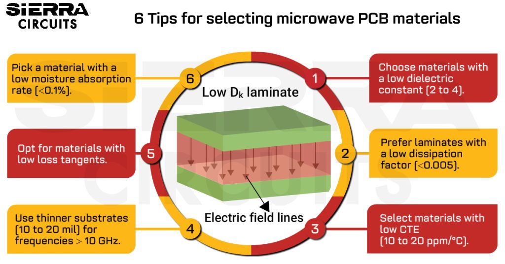
6 factors to consider while selecting RF materials
1. Dielectric constant: Prefer materials with a Dk<4

The dielectric constant is the ratio of a material’s electric permeability to the electric permeability of free space (vacuum). It impacts several key aspects of signal transmission:
- Propagation speed: The material’s dielectric constant determines the speed at which RF signals traverse through it. Higher Dk values result in slower propagation speeds, affecting the signal timing.
- Phase shift: Radio-frequency signals can experience phase shifts as they pass through dielectric materials. The degree of phase shift depends on the material’s Dk.
- Impedance: Impedance is inversely proportional to Dk. Hence, low Dk materials help you achieve uniform impedance for a given trace geometry.
- Coupling: Materials with higher Dk tend to exhibit higher capacitive and inductive coupling between traces, potentially impacting signal quality.
4 parameters that lead to Dk variations
As an RF engineer, you should know the factors that lead to Dk variations to predict the signal behavior during the design phase effectively.
1. Anisotropy
Many PCB base materials exhibit anisotropic behavior, especially those with woven glass cloth. This means their electrical properties, including Dk, differ depending on the measurement direction.
The out-of-plane Dk (measured through the board thickness in the vertical direction) can differ from the in-plane Dk (measured parallel to the board surface in the horizontal direction).
As a result, the Dk value can vary depending on the signal direction, potentially impacting the performance of radio-frequency boards.

2. Operating temperature
Dk is a factor of temperature. As the temperature rises, the Dk value decreases. This can be a concern in high-power applications where heat generation can cause Dk variations. The graph below illustrates how the dielectric constant varies as the temperature rises.

3. Operating frequency
Dk is not constant across the entire frequency spectrum. It typically decreases with an increase in frequency. This phenomenon is known as dispersion. The graph below illustrates how the dielectric constant varies as the frequency rises.

4. Aging
Resins used in RF laminates can undergo environmental degradation over time. Factors such as moisture absorption, thermal cycling, and exposure to harsh operating conditions can hinder the Dk of your material.
Dielectric materials can be categorized into 3 groups based on their Dk values, as shown below:
| Material category | Applications |
|---|---|
| High Dk (>10) | Power amplifier circuits |
| Medium Dk (4 to 10) | Digital communication systems |
| Low Dk (<4) | High-frequency applications like microwave and RF boards |
When choosing materials for RF applications, consider these parameters to ensure reliable electrical performance across the expected temperature range and operating frequency. Refer to the datasheets to understand the Dk variations at specific frequencies and temperatures.
2. Dissipation factor: Choose materials with a Df of <0.005
The dissipation factor (Df) or loss tangent determines the extent of signal loss in a dielectric material. The higher the Df, the higher the signal attenuation.
This attenuation occurs because high-frequency signals rapidly oscillate between positive and negative phases when propagating through a dielectric medium. These signals induce the molecules in the medium to align with the EM field.
Due to molecular cross-linking, the molecules cannot orient themselves to the changing EM field. The continuous oscillation of the high-frequency signal forces molecules to keep moving and generate heat. This increase in temperature leads to energy loss and signal attenuation.
For radio-frequency applications, choose a lower Df (<0.005) material. Dielectric materials can be categorized into 3 groups based on their Df values, as shown below:
| Material category | Applications |
|---|---|
| Low Df (<0.005) | High-speed digital designs, RF and microwave |
| Medium Df (0.005 to 0.02) | Consumer electronic devices |
| High Df (>0.02) | Devices that do not require high electrical performance (e.g. toys) |
3. Insertion loss: Pick low-loss materials and low-profile copper
Insertion loss refers to the overall decrease in signal strength (measured in dB) as it travels through the PCB transmission line.

When choosing RF PC material, you need to consider Df along with other losses present in a circuit.
Insertion loss is essentially the sum of all the individual losses experienced by the signal as it travels from the transmitter to the receiver. This includes conductor, dielectric, radiation, and leakage losses.
Conductor loss
This is the decrease in signal strength in a conductor. Factors such as skin effect, proximity effect, and trace resistance cause this type of signal loss.
The graph below illustrates how high-frequency signals experience greater attenuation as they travel through a transmission line.

To minimize conductor loss, choose materials with low resistivity and employ low-profile copper: very low profile (VLP), hyper very low profile (HVLP), and reverse-treated foil (RTF).
Dielectric loss
Dielectric loss is the energy lost when a signal travels through an insulating material. At higher frequencies, the electric field associated with the signal changes rapidly, causing higher dielectric loss.
To minimize this loss, choose materials with low Dk (<4) and Df (0.005).
The graph below demonstrates materials with a lower Df experience less insertion loss.

Radiation loss
Radiation loss is the phenomenon where EM energy is emitted into free space from the signal lines. As the frequency rises, transmission lines act like antennas, radiating into space. Uncontrolled radiation can interfere with other electronic devices nearby, causing malfunctions and data errors.

Trace bends, vias, or impedance discontinuities can cause the signal to radiate. To reduce this effect, choose low-Dk and thicker substrates. Thicker substrates confine the fields effectively, reducing coupling and radiation loss. The thickness depends on your impedance requirements.
Leakage loss
It is the energy lost due to unintentional current flow through a dielectric material. At very high frequencies, even small leakage currents can contribute to noticeable energy loss.
To prevent current leakage, choose substrates with high volume resistivity (10⁶ – 10¹⁰ MΩ-cm).

For RF boards, selecting a laminate with low Df and smooth copper is advantageous since it reduces the overall insertion loss.
When working with high frequencies, the signal quality can deteriorate due to insertion loss. This can happen because of conflicting dielectric properties, copper profile, and surface finish.
For more details on signal loss analysis, see losses in PCB transmission lines.
4. Coefficient of thermal expansion: Use materials with similar CTEs

CTE measures the expansion rate of a PCB material as it heats up. It is measured in parts per million per degree Celsius [ppm/°C].
The above graphic shows the expansion of a dielectric material in the Z-axis. CTE mismatch occurs when different materials in a hybrid PCB stack-up expand or contract at different rates due to temperature changes.
This can lead to dimensional instability, particularly during drilling and assembly. The amount of tolerable CTE mismatch depends on the specific application requirements and design constraints.
Typically, a lower CTE mismatch is preferred to minimize the risk of mechanical stress, warping, and reliability issues.
How to determine tolerable CTE mismatch
As an RF PCB designer, you need to know the amount of tolerable CTE mismatch in your design. The goal is to choose materials with similar CTEs.
Step 1: Create a table of potential materials.
Step 2: Note each material’s CTE values in the X, Y, and Z axes.
Step 3: Organize the materials in ascending order of CTE mismatch (the smaller the mismatch, the better). i.e. the difference between the CTEs must be as small as possible.
Step 4: Consider additional material properties such as dissipation factor, thermal conductivity, and other relevant thermal properties.
When designing boards for microwave range, select microwave PCB materials that exhibit low CTE (10 to 20 ppm/°C) in the z-axis to maintain dimensional stability under varying temperatures.
5. Thermal conductivity: Opt for materials with higher thermal conductivity
The thermal conductivity (k) indicates the substrate’s ability to disperse heat effectively. The higher the thermal conductivity, the higher the heat dissipation ability.
Typically, k varies between 0.3 W/m-°C and 0.6 W/m-°C, which is relatively lower than copper’s thermal conductivity of 386 W/m-°C. Hence, copper layers in your board dissipate heat more efficiently than dielectric material.

6. Dielectric thickness: Select thickness based on your impedance requirements
Dielectric thickness significantly influences transmission line impedance, especially in high-frequency RF circuits. As dielectric thickness increases, impedance rises.
The material composition (resin type, glass or filler type, and their ratios) determines how well dielectric thickness can be controlled during the PCB fabrication process.
PCB Material Selector tool for RF applications
Pick the best materials that suit your applications instantly with our advanced PCB Material Selector.

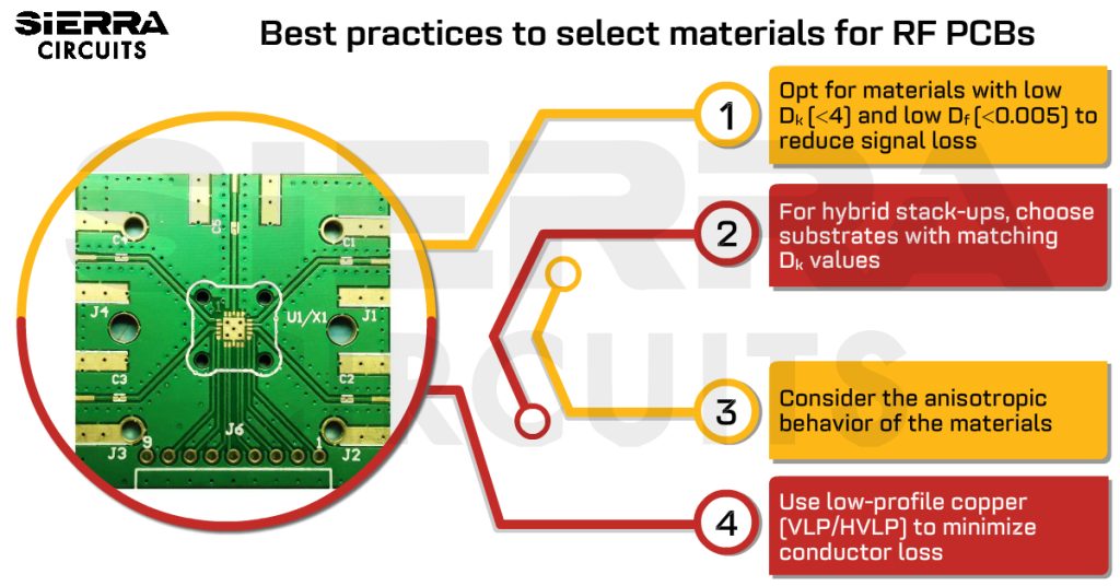
6 best practices to select laminates for radio-frequency PCBs
- Opt for materials with low Dk (<4) and low Df (0.005) to reduce signal loss.
- For hybrid stack-ups, choose materials with matching Dk values.
- Select materials with similar CTEs to avoid functional failures and reliability issues. If the CTE is mismatched, the materials will expand at different rates during the fabrication process.
- Consider the anisotropic behavior of materials and select those with uniform properties in all directions to avoid performance issues.
- Use low-profile copper (VLP/HVLP) to minimize conductor loss and enhance signal transmission quality.
- Choose substrates with high volume resistivity to minimize leakage currents and energy loss at high frequencies.
For more tips on high-speed material selection, download our design guide.
High-Speed Material Design Guide
6 Chapters - 19 Pages - 30 Minute ReadWhat's Inside:
- Importance of choosing the right material for your high-speed design
- Parameters that affect material selection
- Effect of dielectric constituents on your circuit board
- Characteristics of high-speed materials
- Effect of resin content and glass weave structure on your PCB
Download Now
5 fabrication challenges associated with RF materials
The choice of substrate material for radio-frequency PCB not only influences its electrical performance but also impacts the PCB manufacturing process. Here are 5 common challenges your fabricators may face if you choose an incompatible material.
1. Incompatible PCB lamination
RF PCBs may incorporate hybrid stack-ups, which require materials with excellent filling capabilities. The filling materials should be able to flow and fill embedded structures effectively during lamination. This ensures proper encapsulation and minimizes the risk of voids or defects.
Achieving a solid bond during lamination can be difficult as different materials have distinct melt/flow characteristics and respond differently to temperature fluctuations.
Weak bonding between the copper layer and dielectric substrate causes delamination. To avoid this, prefer homogeneous prepregs as they offer excellent adhesion.

Evaluate materials based on their ability to withstand sequential lamination. By carefully considering these factors during material selection, you can ensure an efficient lamination process.
2. Inconsistent scaling in hybrid stack-ups
Scaling in PCB manufacturing is the process of adjusting the size of electronic components, traces, and other features on a PCB layout. The scaling process depends on the material type, thickness, copper weights, and the composition of adjacent layers.
Hybrid stack-ups involve a combination of materials like PTFE, FR4, polyimide, polyimide flex laminates, and bond ply materials. They also have fillers such as ceramic, which can be reinforced or non-reinforced with glass cloths.
During lamination, each material expands at different rates. Precise scaling helps achieve accurate layer-to-layer registration.
At Sierra Circuits, we use the XACT software tool to predict scale values accurately. Adjusting drill parameters based on these calculations ensures accurate layer alignment. Our CAM engineers run an X-ray inspection to detect voids and weak spots.
3. Increased drilling cost
High-density RF stack-ups may require a large number of drilled features, including blind vias, buried vias, and microvias. The selected materials should be compatible with your drilling requirements.

The type of filler used in the material composition can greatly impact the PCB drilling process. Materials containing hard ceramic fillers, such as aluminum oxide or silica, can make drilling more challenging, time-consuming, and expensive.
These hard fillers can cause increased tool wear, slower drilling rates, and higher production costs.
At Sierra Circuits, we implement soft filler particles such as polymeric fillers, PTFE, or specific glass compositions. Soft fillers are generally easier to drill through, resulting in faster drilling rates, reduced tool wear, and lower manufacturing costs.
For more high-density material selection tips, see How to choose the right HDI PCB materials.
4. Incomplete laser ablation
Some RF materials, such as FR4, are well-suited for laser PCB drilling due to their ability to absorb laser energy. However, certain PTFE materials pose significant challenges due to their UV transparency.
Since they don’t absorb the energy, the laser beam passes through them without removing the material, resulting in incomplete drilling.
Our RF PCB designers recently worked on an HDI project that involved drilling microvias on PTFE-based laminates. This required precise control over the laser drilling parameters. Our experts carefully adjusted and monitored the laser wavelength and pulse duration to enhance laser absorption on smooth PTFE surfaces.
Using CO2 laser techniques, we precisely drilled the material, creating microvias with diameters ranging from 50 to 70 micrometers.
For customized RF and microwave PCB design solutions, partner with us.
Book a meeting with our design expert now.
5. Inefficient plating
The chemical composition of the substrate material can affect its compatibility with different plating solutions. Some materials may need specific pre-treatment processes to ensure proper adhesion of the plated metal.
For instance, certain high-performance polymer-based substrates may require additional steps before electroless plating. Consult your CM to understand the compatibility of the chosen substrate material with the intended plating processes.
Sierra Circuits specializes in manufacturing high-quality RF and microwave PCB prototypes. Visit our RF and microwave PCB manufacturing capabilities to get a quote for your radio-frequency prototype today.
Popular RF PCB material types
Polytetrafluoroethylene (PTFE): Also known as Teflon, PTFE is well-known for its low dielectric constant and loss tangent, making it suitable for high-frequency applications. Its exceptional thermal resistance also makes it a dependable choice across various temperatures. PTFE materials generally require high temperatures during fabrication.
Woven glass-reinforced PTFE: These are fabricated using lightweight woven fiberglass and exhibit superior dimensional stability.
Ceramic-filled PTFE: This material improves the mechanical and thermal properties of plain PTFE by combining it with ceramic fillers. It reduces the rate of thermal expansion and increases the dielectric constant while maintaining a low-loss tangent, ensuring good performance across a wider range of frequencies.
Hydrocarbons: These materials are generally more cost-effective than PTFE and perform well in RF applications. Hydrocarbon-based laminates can be customized with specific dielectric and thermal properties to meet design requirements.
Non-PTFE materials: They are generally more affordable than PTFE, making them suitable for cost-sensitive applications. Due to their dimensional stability over a wide frequency range, they are also easier to process and fabricate. However, non-PTFE materials exhibit higher Dk and Df values, increasing the signal loss risk.
Non-PTFE materials such as Astra MT77 and I-Speed are suitable for RF applications.
Key takeaways:
- Choosing the right RF material is crucial for ensuring signal integrity, effective thermal management, uniform impedance, and dimensional stability.
- The dielectric constant influences propagation speed, attenuation, impedance, and coupling. Materials with lower Dk are preferable for achieving better signal transmission.
- Factors leading to Dk variations include anisotropy, operating temperature, operating frequency, and aging.
- Low-profile copper helps reduce overall insertion loss.
- Always make sure the chosen materials are compatible with the intended lamination, drilling, and plating processes.
Always consult your RF PCB manufacturer before finalizing the material to ensure manufacturability and desired board performance. We hope this article helped you choose the right materials for your radio-frequency designs. Let us know in the comments if you need anything else.
Need help designing your RF PCB? Post your questions on SierraConnect, our PCB forum. Our design experts will answer them.


Start the discussion at sierraconnect.protoexpress.com