Contents

On-demand webinar
How Good is My Shield? An Introduction to Transfer Impedance and Shielding Effectiveness
by Karen Burnham
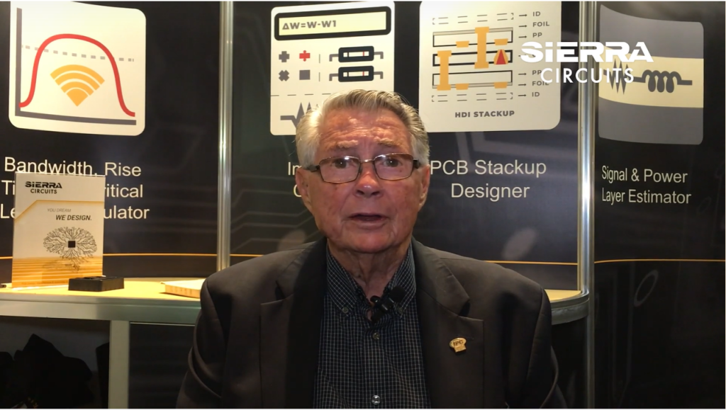
We ran into Vern Solberg of Solberg Technical Consulting at PCB West 2022 and discussed the features of system-in-package. Watch the full video to learn more.
What are flip chip and system-in-package technologies?
Vern Solberg: System-in-package (SiP) technology integrates several devices like semiconductors and passive components into a single package. This facilitates the mounting process on a PCB. For example, a cell phone contains this system that performs all the intended functions.
What is the difference between a flip chip and a wire bond?
Vern Solberg: In a flip chip, the wire bond die is redesigned with metalized bumps to be directly placed on a package substrate. In the wire bond package, the die is placed down and bonded to the package substrate. Usually, gold or thin copper wire connects the terminals of the die to the package. This rerouted wire interacts with circuit boards.
What is die in system-in-package?
Vern Solberg: The die in the package is the semiconductor that performs the desired function. The encasing provides the required mechanical support to the system. You can implement a bare die on a circuit board but there is a size limit. For instance, a very small and delicate die needs reinforcement so it does not crack. Typically, polymers are applied to strengthen both the die and the package substrate.
Why is a die necessary in microelectronics packaging?
Vern Solberg: The die is the base of a microelectronics package that performs the intended function. It could be a processor or a controller, which is the key part of the electronic product. The die will be packaged and tested before mounting.
Can you discuss your semiconductor die and package stacking methodologies?
Vern Solberg: Stacking dies (two or more) can be dated back to the mid-nineties. Nowadays, we can stack around 10 dies in one package. This is a sequential process – bond the first die to a substrate, place the next die on top of it with a spacer in-between, and then wire bond both of them. This is a difficult procedure that does not allow any breakage. You can save space using this method. Stacking is implemented in system-in-package applications such as condensing memory die space.
What is your input on the fanout wafer and panel-level packaging?
Vern Solberg: Metalized silicon wafers are usually referred to as wafer levels. These have conductors that attach and reroute the die terminals to a wider spacing, which is essentially fanout. On the contrary, panel-level technology makes use of a silicon panel, which can be expensive. The alternatives are glass and other stable organic materials. This allows a very fine interconnect between the die and the PCB.
How do flip chips and system-in-package benefit HDI boards?
Vern Solberg: Flip chips are small, two-dimensional, and can be placed side-by-side on a laminate. The die is designed to operate like a system that can be combined and connected to a substrate. Most of the interconnections between the dies are on the packaged substrate, which is mounted on a PCB or BGA.
HDI PCB Design Guide
5 Chapters - 52 Pages - 60 Minute ReadWhat's Inside:
- Planning your stack-up and microvia structure
- Choosing the right materials
- Signal integrity and controlled impedance in HDI
- Manufacturing considerations for higher yields
Download Now
Would you recommend a specific microvia process methodology?
Vern Solberg: This depends on the manufacturer’s capability for laser drilling. It can drill very small vias directly onto the land pad. You have the option of stacking or staggering vias. The stagger process spreads out the concentration of force. Consult your CM for insights, especially on vias like blind and buried vias. They can advise on the most cost-effective and reliable vias to use.
What are your top design guidelines for high-density circuits?
Vern Solberg: Design guidelines are generally specific to materials and the process. I refer to IPC guidelines, which have classifications of classes 1, 2, and 3. Class 3 is more demanding, with finer traces, spaces, and smaller holes. Depending on the yield of the circuit board, the cost can also be high. For alternate guidelines, you can consult your manufacturer. Companies like Sierra Circuits have a lot of guidance documents, and that’s the best place to start.
IPC Class 3 Design Guide
8 Chapters - 23 Pages - 35 Minute ReadWhat's Inside:
- IPC guidelines for manufacturing defects
- IPC standards for assembly processes
- Common differences between the classes
- IPC documents to set the level of acceptance criteria
Download Now
What is the one thing you wish designers remembered about BGA packaging?
Vern Solberg: The limitation of widely used lead-frame devices is that the package size increased with more IOs. But a BGA accommodates more IOs in smaller spaces. We were able to confine all the elements to the package substrate by placing the terminals underneath the die. This was the most practical method of packaging semiconductors that was also compatible with semi-processing. Also, the efficient BGA packaging helped to overcome the coplanarity issues of reframed components.
Vern Solberg is the founder of Solberg Technical Consulting. He has more than 25 years of experience in commercial and aerospace electronic product development. Solberg holds several patents on IC packaging innovations, including the multiple-die and folded-flex 3D package technologies.
If you need to know anything more related to SiP and flip chips please comment below. We will be happy to help you. Check out our design services and let us know if you need any help with your design.


